semi合集-English.pdf - 第5444页
SEMI M60-0305 © SEMI 2005 12 11 Calculations 11.1 Current and C urrent Density 11.1.1 To calculate current(I) from current density(J), multiply the curren t density by the area of gate area(S) as follows: Symbolically: I…
SEMI M60-0305 © SEMI 2005 11
Record Sample ID
Determine Test Parameter
J, T
int
., Tmax,
Δ
V
Probe New Cap.
Set
t
= 0
Measure Vini
Vini
<
Vbd
T > Tmax
Record MOS ID & J
Stop & T
bd
= T
ini
More Cap. on
Wafer?
Report Result
Yes
No
No
Yes
Yes
No
Record MOS ID & J
Stop & T
bd
= Vt
Force J ( I = J/Area)
Wait T
int
.
Measure Vi
Vi
–
Vi-1<
Δ
V
Force J ( I = J/Area)
Wait T
int
.
Record MOS ID
&J stop & T
bd
=
T
max
No
Yes
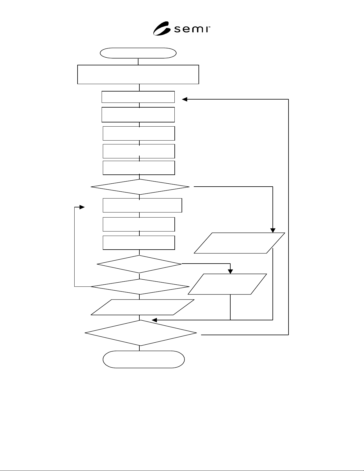
Figure 4
Flow Diagram Outline (2)

SEMI M60-0305 © SEMI 2005 12
11 Calculations
11.1 Current and Current Density
11.1.1 To calculate current(I) from current density(J), multiply the current density by the area of gate area(S) as
follows:
Symbolically:
I = J × S (1)
Example: Given a current density(J) of 1µA/cm
2
and a gate area(S) of 10 mm
2
, the current would be 100nA.
Similarly, compute current density(J, [A/cm
2
]) from measured current(I, [A]) and area (S, [cm
2
]) using.
J = I / S [A/cm
2
] (2)
11.2 Voltage and Electric Field Strength
11.2.1 To calculate voltage(V) from an electric field(E), multiply the electric field strength by the gate oxide
thickness(T
ox
) as follows:
Symbolically:
V = E × T
ox
(3)
where:
T
ox
= Gate oxide thickness, cm.
Example: Given an electric field(E) of 15 MV/cm and a gate oxide thickness(T
ox
) of 25nm, the voltage would be
37.5 V.
Similarly, compute electric field (E, [MV/cm]) from measured voltage(V, [V]) and gate oxide thickness(T
ox
, [cm])
using.
E = V / T
ox
[MV/cm] (4)
11.3 Oxide Voltage
11.3.1 Neglect the flatband voltage shift. The flatband voltage shift is due to gate-substrate work function
difference[
ms
] and oxide fixed charge[Q
f
]. Although it is better to consider this flatband voltage shift, its influence
on the oxide film thickness in the range recommended in this test method is small.
11.4 Calculation of Defect Density
11.4.1 Calculate the defect density using the following equation based on the Poisson distribution assumption of the
dielectric breakdown defects (see Standard EIA/JEDEC 35):
ox
= ln (1 F) / S (5)
Here
ox
= Defect density (defects/cm
2
) ,
F = Failure fraction for each oxide breakdown mode ,
and S = Capacitor gate area (cm
2
).
Example: Given a total of 100 MOS capacitors tested, with 30 accidental-mode-failed capacitors and a gate area of
10 mm
2
, the defect density would be as follows:
ox
= ln ( 1 ( 30 / 100 ) ) / 0.1
= 3.6 defects/cm
2
(6)

SEMI M60-0305 © SEMI 2005 13
11.5 Weibull Distribution
11.5.1 To convert cumulative percent to Weibull format (sometimes referred to as “smallest extreme value
probability distribution III”), use the following equation:
ln ( ln ( 1 F ) ) (7)
11.6 Where ln is the natural log operator and F is a percent of the cumulative failures. Care shall be taken so that F
is never exactly 1 since this will be in an undefined situation.
12 Report
12.1 Report the following for each wafer, as appropriate for the test conditions and as agreed upon by the parties to
the test.
12.1.1 Test Description
12.1.2 Date
12.1.3 Time
12.1.4 Operator
12.1.5 Measurement system ID
12.1.6 Sample lot ID
12.1.7 Wafer ID
12.1.8 Average oxide thickness
12.1.9 Gate area (cm
2
)
12.1.10 Gate material
12.1.11 Oxidation parameters
12.1.12 Type of wafer (Ex: n or p)
12.1.13 Applied stress parameters
12.1.14 Test temperature
12.1.15 Process comment
12.1.16 Capacitor ID such as adress
12.1.17 V-T characteristic data
12.1.18 Breakdown time
12.1.19 Weibull plot of Q
bd
12.1.20 Average, median and maximum Q
bd
12.1.21 Breakdown mode yield
12.1.22 Breakdown mode map or Tbd / Q
bd
map
12.1.23 Result of calculated defect density