semi合集-English.pdf - 第5233页
SEMI M40-0200 © SE MI 2000 15 R1-4.2 Results R1-4.2.1 The average values of each site pattern is reported h ere together with the correspondin g standard deviation. The average m ight be considered as th e characteristic…
SEMI M40-0200 © SEMI 2000 14
would consume many hours, in the case of AFM
(Atomic Force Microscope) many years.
R1-2.2 Techniques based on light scattering are
capable of scanning the entire wafer surface quite
rapidly, in about 1-2 min. Their response function,
however, has a limited spatial bandwidth ranging
approximately from 0.5 to 40 µm. Standards for light
scattering measurements are now emerging (8,9).
R1-2.3 The obvious solution for obtaining a
standardized roughness value of an entire surface is a)
to define a pattern of sites where one- or two-
dimensional scans are performed and b) to report the
significant parameters along with the measurement
(roughness) result. The second task can be solved
theoretically by collecting the important parameters and
by designing an appropriate abbreviation code. The
first task requires experiments to collect data about the
variation of roughness across a typical, real wafer
surface and numerical simulations to find a set of sites
the roughness of which agrees sufficiently well with the
roughness of the entire surface.
R1-2.4 This appendix reports the results of
corresponding roughness measurements as well as of a
numerical simulation using a virtual design-of-
experiment (DOX).
R1-3 Roughness Definitions
R1-3.1 A variety of definitions for roughness have
been standardized by national and international
institutions in the US, Japan and Europe.
Corresponding standards are listed in section 5 of the
main document and some selected ones again in
reference 7. Most widely used are average roughness
R
a
and root-mean-square roughness R
q
. Both refer to
the average deviation of a profile from a reference line.
R1-4 Roughness Measurements
R1-4.1 Experimental Details
R1-4.1.1 Four groups of four wafers each were
investigated to collect data about the variation of
roughness across the wafer surface. The wafers were
selected to represent different process steps and
polishing techniques:
a)
final polished wafers, 150 mm, #1-4
b) final polished wafers, 200 mm, #4-8
c) pre-polished wafers, 200 mm, #9-12
d) acid-etched wafers, 200 mm, #13-16.
R1-4.1.2 The wafers were characterized for haze with
an SSIS (Censor ANS-100) and the roughness
measurements were performed with an optical non-
contact profiler (Chapman MP-2000+). The roughness
data were taken by performing scans of length 3 mm
and were evaluated using filters of 19, 30, 80 and 250
µm, respectively. The scans were performed at a
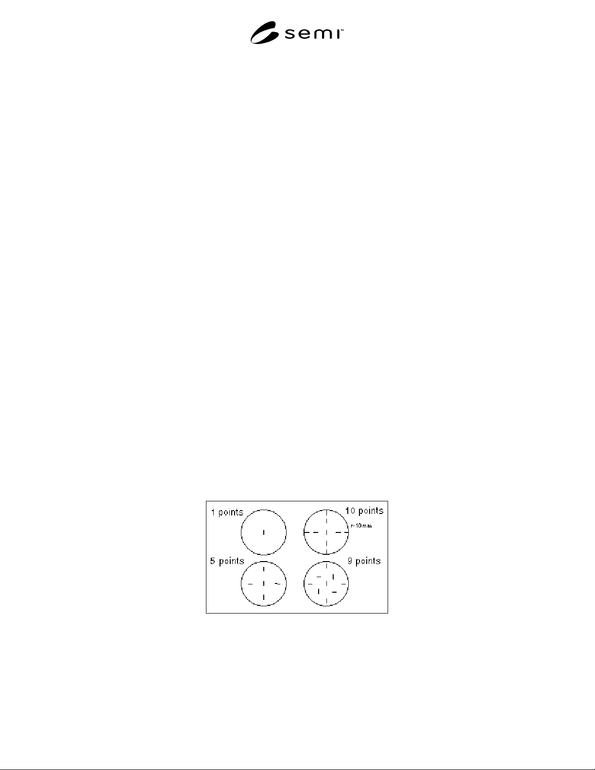
variety of sites according to four different site patterns
as displayed in Figure R1-1 where also the directions of
the various scans are indicated:
i) center of wafer, one scan
ii) five points, center of wafer plus four points at 2/3
of radius
iii) nine points, center of wafer plus four points at 2/5
of radius plus four points at 4/5 of radius
iv) ten points, two in the center of wafer plus four
points at ½ of radius and four points at radius
minus 10 mm.
v) thirteen points, combination of pattern ii and iii.
Figure R1-1
Site Patterns
SEMI M40-0200 © SEMI 200015
R1-4.2 Results
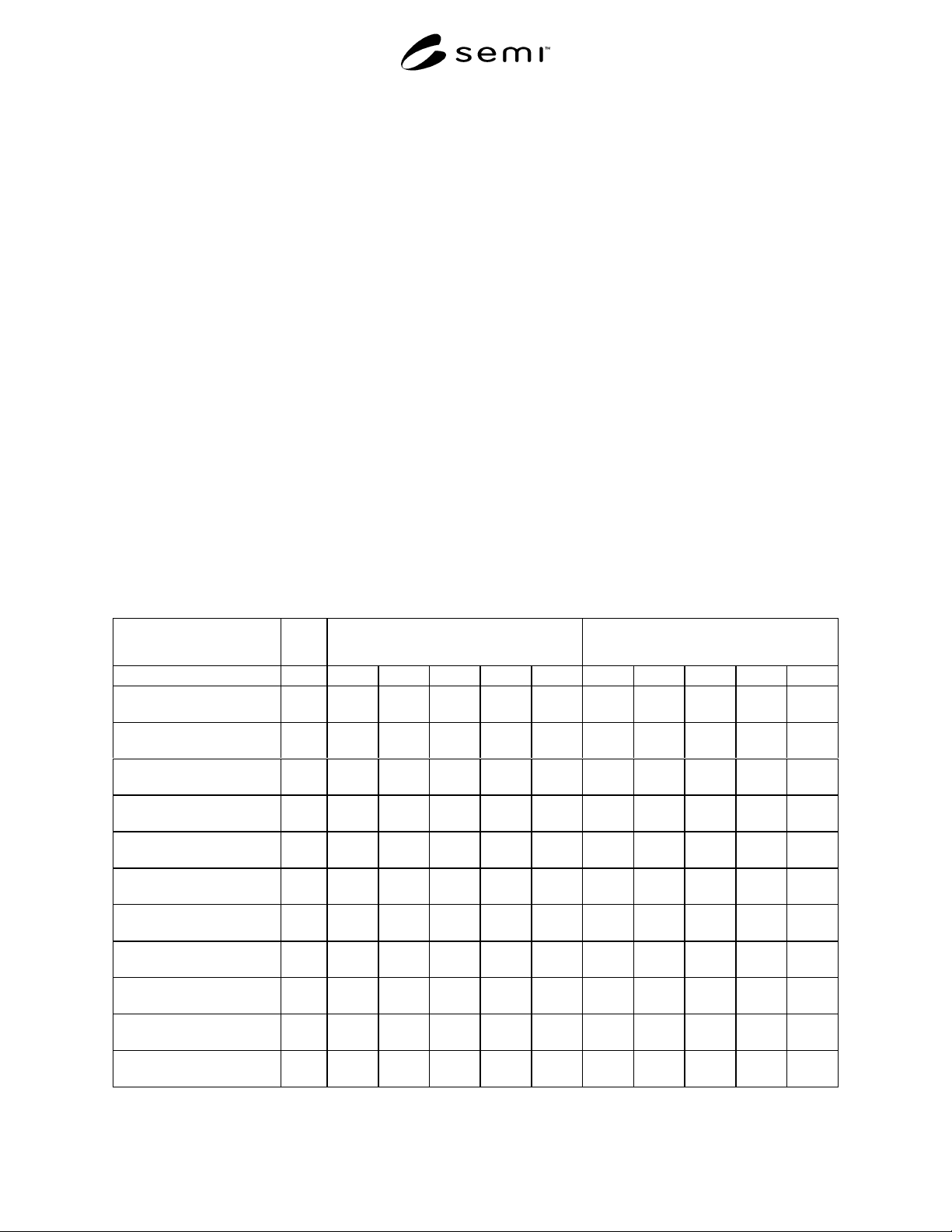
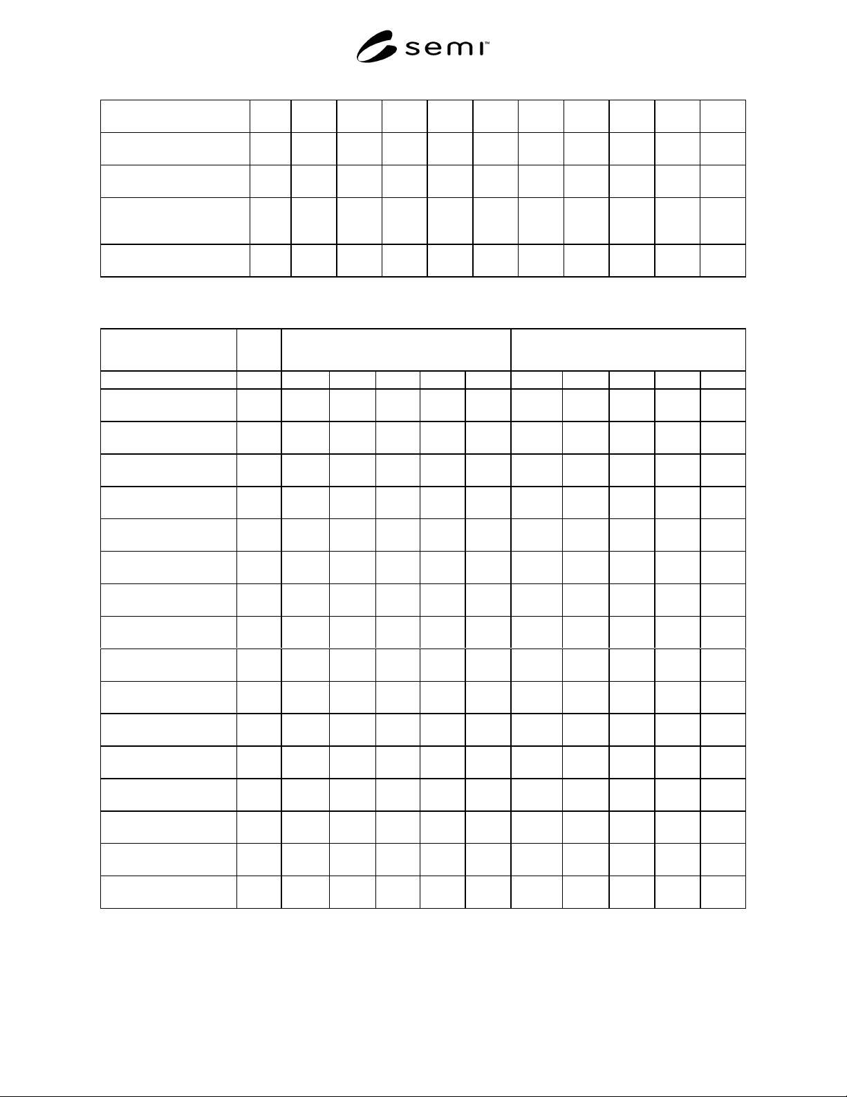
R1-4.2.1 The average values of each site pattern is reported here together with the corresponding standard
deviation. The average might be considered as the characteristic roughness of the entire surface whereas the
standard deviation is a measure of roughness inhomogeneity. The results are summarized in Tables R1-1 and R1-3.
These averages and standard deviations are called site average or site standard deviation for the respective site
patterns for each wafer and each filter length applied.
R1-4.2.2 The variation in average values obtained with the different site patterns employed can be obtained by
calculating 1) the average ofthe individual site averages and the standard deviation for each wafer and 2) the average
of the individual site standard deviations and the corresponding standard deviation. These averages are called wafer
average and wafer standard deviation, respectively. The corresponding standard deviations are called standard
deviation of wafer average and standard deviation of wafer standard deviation. They are reported in Table R1-3 and
Table R1-5 and in Figure R1-2 and Figure R1-3.
R1-4.2.3 The site average roughness values found range from 0.09 A for final polished wafers to 350 A for acid
etched wafers for a 10 µm filter and from about 5 A to 2200 A, respectively, for a 250 µm filter. In total, a range of
about four and a half orders of magnitude is covered. The site standard deviation for the different site patterns is
around 10-15% of the average roughness of the wafer indicating a homogeneous roughness of the wafer surfaces.
The difference between the site patterns ii, iii, iv and v for the relative site standard deviation is small, typically
about 1-2 %. Exceptions are for the 200 mm final polished wafers with standard deviations of about 50-60% for the
10 µm filter.
R1-4.2.4 According to the values in Tables R1-3 & R1-5, the standard deviations of the wafer averages are less than
10 % in any case (Figure RI). The standard deviations of the various site standard deviations (Figure A3) are also
smaller than or about 10 % with respect to the wafer average. This indicates that in the present case any site pattern
—with the exception of the single site measurement at the wafer center—represents the “true” mean roughness of
the entire surface and its standard deviation reasonably well.
Table R1-1 Results of Roughness Measurements, 10 and 30 µm Filters
Wfr # Average/Standard Deviation, A
10 µm Filter
Average/Standard Deviation, A
30 µm Filter
Site pattern i ii iii iv v i ii iii iv v
Final polished, 150 mm 1 0.08 0.086/
0.005
0.089/
0.009
0.090/
0.007
0.086/
0.008
0.36 0.390/
0.020
0.396/
0.030
0.389/
0.028
0.396/
0.025
2 0.09 0.090/
0.007
0.094/
0.010
0.090/
0.005
0.093/
0.009
0.43 0.408/
0.037
0.413/
0.035
0.410/
0.028
0.410/
0.035
3 0.09 0.090/
0.000
0.092/
0.008
0.090/
0.005
0.092/
0.007
0.41 0.404/
0.018
0.401/
0.030
0.387/
0.022
0.402/
0.027
4 0.09 0.090/
0.000
0.097/
0.010
0.090/
0.004
0.095/
0.009
0.40 0.402/
0.015
0.420/
0.025
0.414/
0.016
0.415/
0.024
Final polished, 200 mm 5 0.23 0.14/
0.05
0.15/
0.06
0.15/
0.06
0.14/
0.06
1.17 0.746/
0.35
0.827/
0.33
0.795/
0.32
0.769/
0.29
6 0.26 0.13/
0.07
0.15/
0.06
0.15/
0.06
0.14/
0.06
1.36 0.746/
0.35
0.846/
0.36
0.801/
0.33
0.768/
0.32
7 0.10 0.13/
0.03
0.12/
0.04
0.13/
0.06
0.13/
0.04
0.53 0.736/
0.23
0.699/
0.23
0.752/
0.32
0.726/
0.22
8 0.09 0.12/
0.02
0.11/
0.02
0.12/
0.03
0.12/
0.02
0.50 0.648/
0.15
0.626/
0.14
0.636/
0.18
0.644/
0.13
Pre-polished, 200 mm 9 2.64 2.41/
0.25
2.45/
0.32
2.39/
0.39
2.42/
0.29
7.21 6.398/
0.77
6.538/
0.83
6.387/
0.91
6.432/
0.78
10 2.64 2.56/
0.36
2.69/
0.19
2.37/
0.41
2.64/
0.27
6.84 6.760/
0.95
7.147/
0.50
6.419/
1.00
7.022/
0.27
11 2.75 2.77/
0.07
2.78/
0.10
2.46/
0.45
2.78/
0.09
7.30 7.310
0.19
7.302/
0.30
6.545/
1.05
7.305/
0.27
SEMI M40-0200 © SEMI 2000 16
12 2.76 2.48/
0.32
2.50/
0.32
2.43/
0.42
2.47/
0.31
7.30 6.566/
0.91
6.521/
0.75
6.146/
1.05
6.478/
0.77
Acid etched, 200 mm 13 327.2 332.0/
6.73
335.0/
16.25
352.6/
12.37
334.5/
13.76
826.2 873.5/
43.16
869.5/
50.22
906.5/
28.56
874.4/
46.13
14 337.9 344.9/
18.74
344.7/
9.19
353.1/
12.11
345.3/
13.00
876.8 899.9/
60.49
915.5/
24.15
930.0/
43.19
912.5/
39.69
15 339.5 340.5
8/13.4
2
335.2/
6.07
363.4/
7.22
337.0/
9.58
887.7 913.7/
68.10
879.1/
24.64
966.1/
30.75
891.7/
47.65
16 337.6 331.8/
8.84
337.6/
13.37
348.7/
9.26
335.4/
12.41
922.8 886.1/
37.57
896.0/
38.04
921.8/
27.16
890.2/
37.14
Table R1-2 Results of Roughness Measurements, 80 and 250 µm Filters
Wfr. # Average/Standard Deviation, A
80 µm filter
Average/Standard Deviation, A
250 µm filter
Site pattern i ii iii iv v i ii iii iv v
Final polished, 150 mm 1 1.33 1.426/
0.075
1.416/
0.134
1.434/
0.108
1.426/
0.115
4.34 4.678/
0.484
4.836/
0.632
4.786/
0.435
4.813/
0.578
2 1.57 1.470/
0.112
1.482/
0.147
1.444/
0.112
1.471/
0.133
5.34 4.944/
0.312
5.441/
0.613
4.592/
0.434
5.258/
0.591
3 1.49 1.460/
0.025
1.472/
0.131
1.357/
0.080
1.466/
0.108
4.81 4.788/
0.403
5.164/
0.823
4.353/
0.507
5.047/
0.735
4 1.33 1.394/
0.089
1.446/
0.115
1.461/
0.069
1.435/
0.106
4.09 4.528/
0.619
4.814/
0.584
4.934/
0.503
4.760/
0.585
Final polished, 200 mm 5 3.29 2.582/
0.45
2.638/
0.71
2.531/
0.65
2.566/
0.60
7.33 6.676/
0.45
6.627/
0.99
6.560/
0.95
6.592/
0.82
6 3.65 2.560/
0.65
2.724/
0.79
2.510/
0.67
2.590/
0.69
7.49 6.804/
0.57
6.834/
0.93
6.443/
0.92
6.772/
0.80
7 2.02 2.682
/0.72
2.493/
0.56
2.641/
0.81
2.602/
0.61
5.45 6.914/
1.37
6.601/
0.81
7.057/
1.47
6.810/
0.97
8 1.97 2.400/
0.45
2.317/
0.40
2.279/
0.54
2.375/
0.40
5.56 6.268/
0.59
6.342/
0.69
6.232/
1.08
6.374/
0.62
Pre-polished, 200 mm 9 11.12 9.94/
1.06
10.19/
1.09
10.10/
1.27
10.02/
1.04
15.15 14.25/
1.31
14.50/
1.18
14.47/ 14.36/
1.22
10 10.13 10.54/
1.34
11.05/
0.78
10.27/
1.35
10.92/
1.03
14.40 15.44/
2.01
15.58/
0.77
14.59/
1.88
15.62/
1.28
11 11.29 11.35/
0.31
11.26/
0.45
10.13/
1.23
11.29/
0.41
15.75 16.56/
0.59
16.27/
0.81
14.83/
1.26
16.42/
0.74
12 10.60 10.11/
1.10
9.86/
0.95
9.92/
1.12
9.90/
0.99
14.42 14.33/
1.31
14.10/
1.14
14.41/
1.26
14.17/
1.21
Acid etched, 200 mm 13 1257.0 1404/
140.8
1391/
123.44
1439/
88.10
1406/
122.83
1789.6 2127/
331.59
2118/
295.83
2185/
270.70
2147/
291.78
14 1421.9 1460/
109.9
1514/
53.27
1497/
95.92
1501/
78.94
2154.6 2256/
154.21
2366/
222.41
2322/
216.72
2349/
203.72
15 1374.7 1500/
199.2
1396/
94.33
1549/
95.25
1438/
147.56
1970.4 2350/
508.52
2071/
257.41
2348/
198.70
2186/
384.36
16 1478.4 1421/
109.9
1450/
108.89
1477/
104.51
1437/
109.71
2006.4 2075/
186.85
2219/
297.40
2264/
252.44
2180/
271.75
R1-4.2.5 The five-point site pattern appears to represent the average surface reasonably well for wafers where the
roughness does not vary more than by a factor of about two across the entire surface. Patterns with a higher number
of sites are recommended for problematic surfaces.