semi合集-English.pdf - 第7412页
SEMI MF1527-1104 © SEMI 2003, 2004 18 R2-3.1 Diameter Correction Factor —For measure- ments at the center of a circ ular wafer, this factor is given as a function of the rat io of the average pro be-tip spacing, S , to t…

SEMI MF1527-1104 © SEMI 2003, 2004 17
RELATED INFORMATION 2
ERRORS IN RESISTIVITY DETERMINATION BY THE FOUR-POINT
PROBE METHOD (SINGLE CONFIGURATION) RESULTING FROM
UNCERTAINTIES IN WAFER DIAMETER, WAFER THICKNESS, AND
PROBE-TIP SPACING
NOTICE: This related information is not an official part of SEMI MF1527. It was derived from
information developed during the original preparation of the standard in ASTM Committee F-1 in 1994.
This related information was approved for publication by the Silicon Wafer Committee on July 15, 2004.
R2-1 The resistance of an infinitely thin uniform sheet
of infinite extent as measured with an equal spaced, in-
line four-point probe is given as follows:
2ln
m
s
I
V
(R2-1)
where:
s
=
resistance of the infinite sheet, , and
(V/I)
m
= average of the forward and reverse voltage-
current ratios, .
The resistivity of the sheet can be obtained by
multiplying the sheet resistance by the sheet thickness
as follows:
w
s
4
10
(R2-2)
where:
=
resistivity, ·cm,
s
=
resistance of the infinite sheet, , and
w =
thickness, m.
R2-2 Corrections to this equation can be made to
obtain the resistivity of a wafer that has finite thickness
and diameter, as measured with a four-point probe with
slightly unequal probe-tip spacings with an average
value of
S at a temperature slightly different from the
reference temperature. The general solution to this
problem must take account of its three-dimensional
aspect. Solutions are available for the case of a semi-
infinite medium or for an infinitely thin sheet. If the
deviation from the thin sheet approximation is
sufficiently small, the correction factors can be
determined from independent solutions of two-
dimensional electrostatic problems and multiplied
together as follows:
Tsp
m
C
FF
D
S
F
S
w
wF
I
V
2ln
10
4
23
(R2-3)
where:
23°C
= wafer resistivity at a reference temperature
of 23°C, ·cm,
w =
wafer thickness, m,
(V/I)
m
= average of the forward and reverse voltage-
current ratios, ,
F(
S /D)
= correction factor to account for finite wafe
r
diameter (see Section R2-3.1),
S
= average probe-tip spacing, mm,
D = wafer diameter, mm,
F(w/
S
)
= correction factor to account for finite wafe
r
thickness (see Section R2-3.2),
F
sp
= correction factor to account for slightly
unequal probe-tip spacings (see Section R2-
3.3), and
F
T
= correction factor to account for differences
b
etween measurement and reference
temperature.
NOTE 1: The correction factor F
2
in SEMI MF84 is equal to
F( S /D)/ln 2.
R2-3 The relative variation in resistivity for small
variations in these factors is given by the following
relationship:
14
T
T
sp
sp
C
C
F
F
F
F
DSF
DSF
SwF
SwF
w
w
I
I
V
V
d
d
)/(
)/(d
)/(
)/(d
ddd
d
23
23
(R2-4)
The relative variations of the correction factors
F(w/
S ), F( S /D), and F
sp
may be related to variations
in wafer diameter, wafer thickness, and probe-tip
spacing as follows:
14 Bullis, W. M., “Standard Measurements of the Resistivity of
Silicon by the Four-probe Method,” NBSIR 74-496 (August 1974),
73 pp. Available from the National Technical Information Service,
Springfield, VA 22161, as COM 74-11576.

SEMI MF1527-1104 © SEMI 2003, 2004 18
R2-3.1 Diameter Correction Factor—For measure-
ments at the center of a circular wafer, this factor is
given as a function of the ratio of the average probe-tip
spacing, S , to the diameter, D, as follows:
15
3)/(
3)/(
ln2ln
2ln
)/(
2
2
DS
DS
DSF
(R2-5)
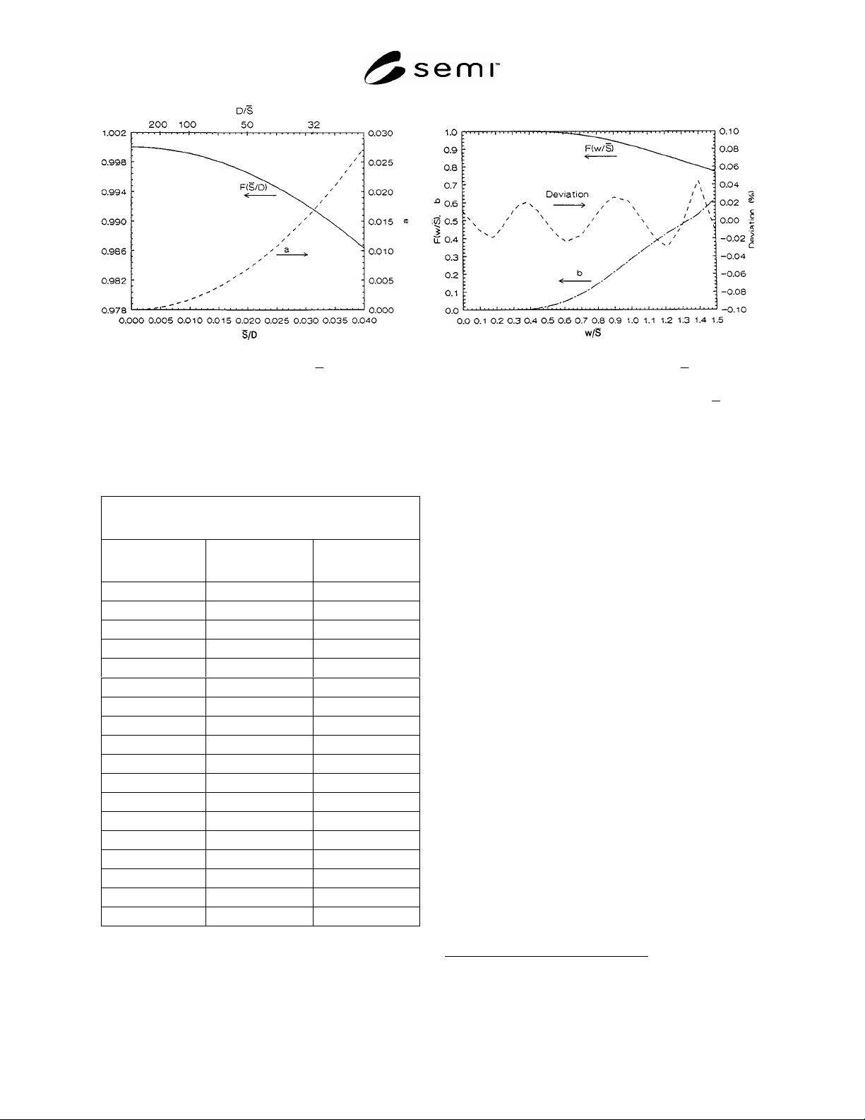
This factor is plotted in Figure R2-1 for
S /D ratios
from 0 to 0.04, which includes all practical ratios for
wafers of diameter 50.8 mm (2.00 in.) and up for
probes with average probe-tip spacing of 0.635 mm
(0.025 in.) to 1.588 mm (0.0625 in.). These ratios
range from 0.00212 for a 300-mm diameter wafer and a
probe-tip spacing of 0.635 mm to 0.03125 for a 50.8-
mm diameter wafer and a probe-tip spacing of 1.588
mm.
R2-3.1.1 Over this range, the factor can be fitted to
better than 0.001% with the following fourth-order
polynomial:
53
25
)/(841714.70)/(181781.0
)/(657959.8)/(104887.1
000000.1)/(
DSDS
DSDS
DSF
(R2-6)
R2-3.1.2 The effect of variation in S or D on F ( S
/D) is given as follows:
S
S
a
D
D
a
DS
DSF dd
)/(F
)/(d
(R2-7)
where:
D
S
DS
DSF
DSF
a
)/(
)/(
)/(
1
R2-3.1.3 The coefficient, a, is also plotted in Figure
R2-1. It is sufficiently small that this source of error
can be neglected in all practical cases.
R2-3.2 Thickness Correction Factor—This factor is a
slowly converging infinite series that was tabulated by
Smits
15
based on a calculation method developed by
Uhlir.
16
A relatively efficient formula
17
for calculating
15 Smits, F. M., “Measurement of Sheet Resistivities with the Four-
point Probe,” Bell Sys. Tech. J. 37, 711–718 (1958).
16 Uhlir, A., Jr., “The Potentials of Infinite Systems of Sources and
Numerical Solutions of Problems in Semiconductor Engineering,”
Bell Sys. Tech. J. 34, 105–127 (1958)
17 Phillips, W. E., “Correction Factor for Finite Thickness,” in
Methods of Measurement for Semiconductor Materials, Process
Control and Devices: Quarterly Report, October 1 to December 31,
1970, NBS Technical Note 592, W. M. Bullis, Ed., August 1971, pp.
9–11. Available from the National Technical Information Service,
Springfield, VA 22161, as AD 728611.
this factor,
)/( SwF , is given in Related Information 1
of SEMI MF84; the result is plotted in Figure R2-2 over
the range of
Sw/ from 0 to 1.5, which covers all
practical measurements of standard sized wafers as
specified in SEMI M1. Over this range, the factor may
be approximated to better than ±0.04% by a sixth-order
polynomial as follows:
6
54
32
)/(154327.0
)/(684549.0)/(001842.1
)/(461693.0)/(069677.0
)/(001130.0000107.1)/(
Sw
SwSw
SwSw
SwSwF
(R2-8)
R2-3.2.1 The effect of variations in w or
S on
)/( SwF is given as follows:
w
w
b
S
S
b
SwF
SwF dd
)/(
)/(d
(R2-9)
where:
.
)/(
)/(
)/((
1
S
w
Sw
SwF
SwF
b
R2-3.2.2 The coefficient, b, is also plotted in Figure
R2-2 together with the percent deviation of the
polynomial fit (Eq. R2-8) from
)/( SwF . The
oscillations due to the polynomial fit can be seen in the
plots of both b and the percent deviation. However, the
curve for b calculated from the derivative of the
polynomial fit provides a reasonable estimate of its
magnitude. It can be seen that the coefficient, b,
becomes rather large when w/ S is greater than about 1
that occurs when large diameter wafers (w 0.625 mm)
are measured with a four-point probe with probe
spacing of 0.635 mm (0.025 in.).
R2-3.3 Probe-Tip Spacing Correction Factor—When
the probe-tip spacings differ from their mean value,
S ,
by only a few percent, this factor is given
approximately as follows:
14
S
S
F
sp
2
1082.11 (R2-10)
where:
S
2
= the spacing between the inner two probes, mm.
R2-3.3.1 The effect of variations in S
2
or
S on F
sp
is
given as follows:
2
2
d
082.1
d
082.1
d
S
S
S
S
F
F
sp
sp
(R2-11)
SEMI MF1527-1104 © SEMI 2003, 2004 19
Figure R2-1 Figure R2-2
Diameter Correction Factor, F(
S /D), and Thickness Correction Factor, F(w/ S ), Error
Error Coefficient, a Coefficient, b, and Percentage Deviation
between Fit (Equation R2-7) and F(w/
S )
R2-3.3.2 Uncertainty in probe-tip spacing arises both
from the error in measurement and from probe-tip
wander.
R2-4 Temperature Correction Factor—SEMI MF84
requires that the resistivity of a silicon wafer be
corrected to its value at 23°C. Between 18° and 28°C,
the resistivity of silicon can be treated as a linear
function of the temperature; over this temperature
range, the temperature correction factor, F
T
is given as
follows:
)23(1
TCF
TT
(R2-12)
where:
C
T
= temperature coefficient of resistivity,
(·cm)/(·cm·°C), and
T = temperature, °C, at which the resistivity
measurement was made.
R2-4.1 The temperature coefficient has been deter-
mined experimentally as a function of the resistivity of
both boron- and phosphorus-doped silicon.
18
As
outlined in SEMI MF84, the experimental data have
been fitted with polynomials of the form:
k
n
n
nT
AC
0
)(ln
(R2-13)
where:
A
n
= the appropriate coefficients (see Table R2-1),
=
wafer resistivity, ·cm, and
k = 17 for phosphorus-doped silicon and 13 for boron-
doped silicon.
R2-4.2 These polynomials are such that nowhere
within the resistivity range 0.001 and 500 ·cm does
the value of C
T
derived from them deviate from the
18 Bullis, W. M., Brewer, F. H., Kolstad, C. D., and Swartzendruber,
L. J., “Temperature Coefficient of Resistivity of Silicon and
Germanium Near Room Temperature,” Solid-State Electron. 11, 639–
646 (1968).
Table R2-1 Polynominal Coefficients for
Temperature Coefficient of Resistivity, %/°C
Coefficient
Phosphorus-Doped
Silicon
Boron-Doped
Silicon
A
0
7.364 × 10
1
7.068 × 10
1
A
1
6.560 × 10
2
8.544 × 10
2
A
2
3.075 × 10
2
1.478 × 10
2
A
3
2.427 × 10
3
1.635 × 10
3
A
4
7.5883 × 10
3
2.003 × 10
3
A
5
7.5541 × 10
4
3.415 × 10
4
A
6
1.39760 × 10
3
2.0915 × 10
4
A
7
1.159 × 10
6
4.3237 × 10
5
A
8
1.106882 × 10
4
7.0532 × 10
6
A
9
4.56719 × 10
6
1.60868 × 10
6
A
10
4.407686 × 10
6
1.0346 × 10
7
A
11
2.601512 × 10
7
2.5201 × 10
8
A
12
9.408560 × 10
8
5.6419 × 10
10
A
13
6.190700 × 10
9
1.4445 × 10
10
A
14
1.032377 × 10
9
A
15
6.890181 × 10
11
A
16
4.58514 × 10
12
A
17
2.94332 × 10
13