semi合集-English.pdf - 第7903页
SEMI T13.2-1104 © SEMI 2004 23 Cl ie n t (H TT P C l i en t ) Bro k e r (H TT P Se r v er ) HT T P P O S T < M e s sa g e C1 > HT T P 20 0 < A c k n o w le dg e > Cl i e n t (H T T P C l i ent ) Br o ke r (H …
SEMI T13.2-1104 © SEMI 2004 22
RELATED INFORMATION 1
IPC MESSAGING MECHANISM AND STRUCTURE
NOTICE: This related information is not an official part of SEMI T13.2 and was derived from the Japanese
Traceability Committee. This related information was approved for publication by full letter ballot on July 23,
2004.
R1-1 HTTP and SOAP Envelope
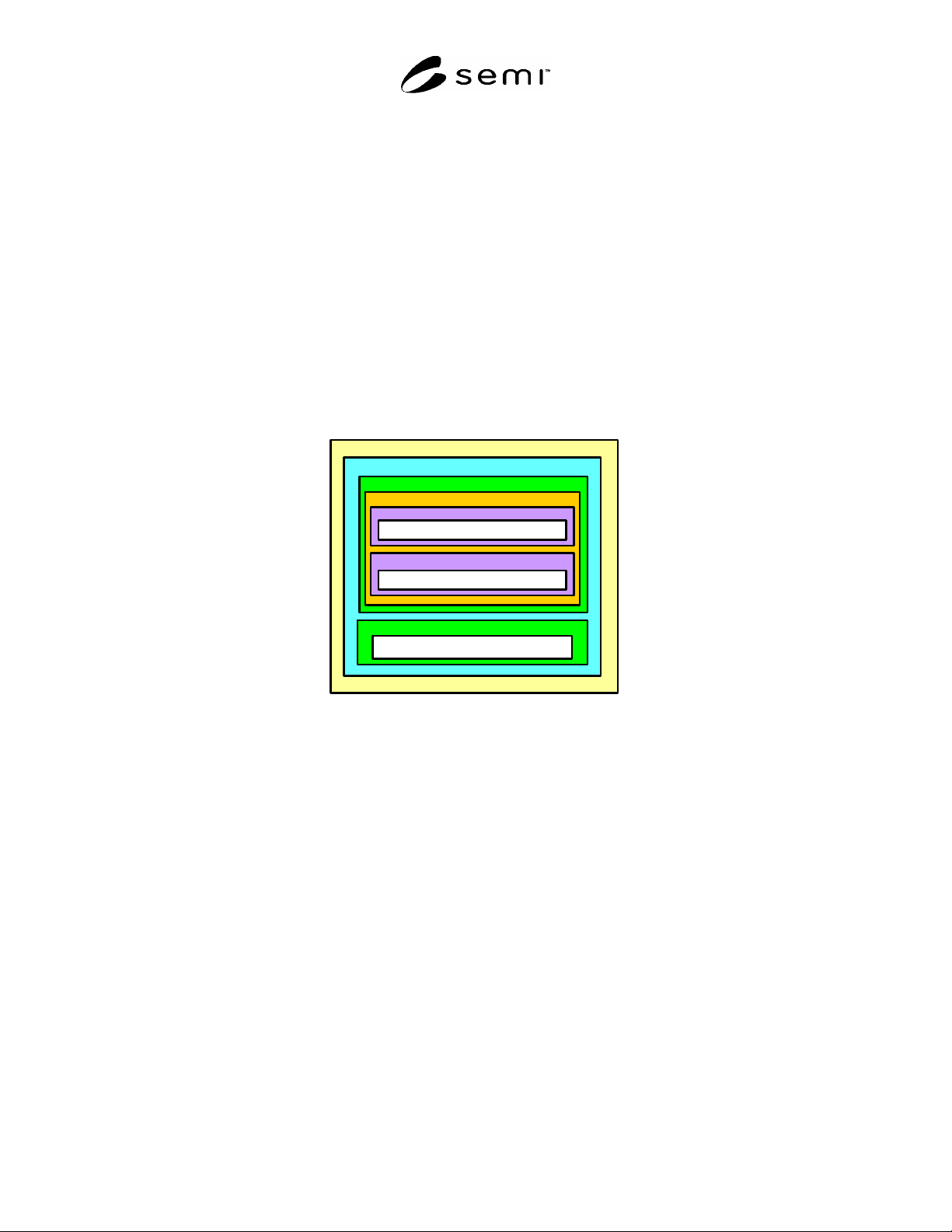
R1-1.1 The following diagram illustrates HTTP message border and SOAP Envelope structure. SOAP Header
contains information of the message and SOAP body just contains SOAP Faults to make sure what happens when
something wrong. Intended message service and its parameters are contained in second MIME Block to make it
possible to allow mixture of non-XML data.
R1-2 Communication with Message Broker
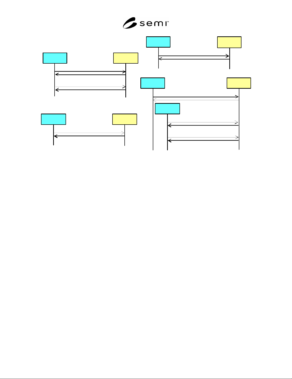
R1-2.1 The following diagrams show client-server communications with Message Broker.
HTTP 1.1
SOAP with MIME Envelope
MIME Block
MIME Block
Mess age Name a nd Parameters
SOAP Envelope
SOAP Body
SOAP Header
SOAP Faults
Me s s ag e I n f o r ma t i on
Figure R1-1
SOAP Envelope and MIME Blocks
SEMI T13.2-1104 © SEMI 2004 23
Client
(HTT P Clien t)
Broker
(HTT P Se rver)
HTTP POST <MessageC1>
HTTP 200 <Acknowledge>
Client
(HTTP Client)
Broker
(HTT P Serve r)
HTT P POST < getM essag e>
HTTP 200 <MessageB1>
Client
(HTTP Client)
Br oker
(HTTP Serve r)
HTTP POST <g etMessage >
HTTP 200 <empty>
HTTP POST <Ack nowledge>
HTTP 200 <empty>
Client
(HTT P Clien t)
Broker
(HTT P Serve r)
HTTP POST <M essa geC2>
HTTP 200 <Ackno wledge>
Client
(HTTP Client)
HTTP POST <getMessage>
HTTP 200 <MessageC2>
HTTP P OST <Ackn owledge>
HTTP 200 <empty>
Message from Client to Broker
Message from Broker to Client
No Message from Broker to Client
Messa
g
e between Client
s
Figure R1-2
Communication with Message Broker
NOTICE: SEMI makes no warranties or representations as to the suitability of the standards set forth herein for any
particular application. The determination of the suitability of the standard is solely the responsibility of the user.
Users are cautioned to refer to manufacturer's instructions, product labels, product data sheets, and other relevant
literature, respecting any materials or equipment mentioned herein. These standards are subject to change without
notice.
By publication of this standard, Semiconductor Equipment and Materials International (SEMI) takes no position
respecting the validity of any patent rights or copyrights asserted in connection with any items mentioned in this
standard. Users of this standard are expressly advised that determination of any such patent rights or copyrights, and
the risk of infringement of such rights are entirely their own responsibility.
Copyright by SEMI® (Semiconductor Equipment and Materials
International), 3081 Zanker Road, San Jose, CA 95134. Reproduction of
the contents in whole or in part is forbidden without express written
consent of SEMI.

SEMI T14-1104 © SEMI 2004 1
SEMI T14-0705
SPECIFICATION FOR MICRO ID ON 300 mm SILICON WAFERS
This specification was technically approved by the Global Traceability Committee and is the direct
responsibility of the Japanese Traceability Committee. Current edition approved by the Japanese Regional
Standards Committee on July 23, 2004. Initially available at www.semi.org September 2004; to be published
November 2004.
NOTICE: The designation number of T14 was updated during the 0705 cycle to reflect the creation of T14.1
1 Purpose
1.1 The purpose of this document is to specify a new means of identification with the Micro ID on 300mm polished
monocrystalline Silicon wafer with polished edge for process control.
1.2 The objective of the Micro ID is to keep unique information to be assigned in the device manufacturing process
on the location defined on the wafer bevel.
2 Scope
2.1 This document assumes that the Micro ID is implemented under the responsibility of Device Manufacturers.
2.2 A two-dimensional data matrix code symbol consists of the microdots marked on the bevel of a semiconductor
wafer.
2.3 Although this specification does not specify the marking techniques that may be employed when complying
with its requirements, it is assumed that the microdots will be obtained by laser irradiated individual dots.
2.4 The data matrix code symbol is applicable to a broad range of wafer products (un-patterned or patterned wafers)
with mirror polished
bevel surface.
2.5 The format and algorithms of this code are based on two-dimensional symbology specified in ISO/IEC ISS
16022.
NOTICE: This standard does not purport to address safety issues, if any, associated with its use. It is the
responsibility of the users of this standard to establish appropriate safety health practices and determine the
applicability or regulatory limitations prior to use.
3 Referenced Standards
3.1 SEMI Standards
SEMI AUX001 — List of Vendor Identification Codes
SEMI M1 ― Specifications of Polished Monocrystalline Silicon Wafers
SEMI M1.15 — Standard for 300 mm Polished Monocrystalline Silicon Wafers (Notched)
SEMI T1 — Specifications for Back Surface Bar Cord Marking of Silicon Wafers
SEMI T7 — Specification for Back Surface Marking of Double-Side Polished Wafers with a Two-Dimensional
Matrix Code Symbol
3.2 ISO
1
/IEC
2
Standard
ISO/IEC ISS 16022 — Information Technology – International Symbology Specification – Data Matrix
NOTICE: Unless otherwise indicated, all documents cited shall be the latest published versions.
1 International Organization for Standardization, ISO Central Secretariat, 1, rue de Varembé, Case postale 56, CH-1211 Geneva 20, Switzerland.
Telephone: 41.22.749.01.11; Fax: 41.22.733.34.30, Website: /www.iso.ch
2 International Electrotechnical Commission, 3, rue de Varembé, Case Postale 131, CH-1211 Geneva 20, Switzerland. Telephone:
41.22.919.02.11; Fax: 41.22.919.03.00, Website: www.iec.ch