semi合集-English.pdf - 第7579页
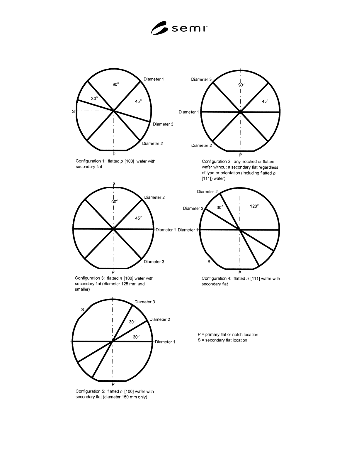
SEMI MF2074-1103 © SEMI 2003 2 7 Keywords 7.1 diameter, sem iconductor, silicon, wafer Figure 1 Diameter Measurement Positions by Wafer Fiducials Categor y

SEMI MF2074-1103 © SEMI 2003 1
SEMI MF2074-1103
GUIDE FOR MEASURING DIAMETER OF SILICON AND OTHER
SEMICONDUCTOR WAFERS
This standard was technically approved by the Global Silicon Wafer Committee and is the direct
responsibility of the North American Silicon Wafer Committee. Current edition approved for publication by
the North American Regional Standards Committee on September 3, 2003. Initially available at
www.semi.org October 2003; to be published November 2003. Originally published by ASTM International
as ASTM F 2074-00. Last previous edition ASTM F 2074-00.
1 Purpose
1.1 The diameter of semiconductor wafers is an
important parameter in microelectronic fabrication.
Wafer diameters must conform to the limits specified in
SEMI M1; or other agreed upon limits, or product that
is otherwise suitable may not fit correctly in process
equipment.
1.2 Cam-follower edge rounding usually results in
wafers that are circular. However, wafers ground with
edge-follower edge rounding equipment may be
elliptically shaped. Measurements made at the three
positions specified in this guide do not provide
complete information about the roundness of the wafer.
2 Scope
2.1 This guide defines standardized positions for
measuring diameter of circular wafers of silicon and
other semiconducting materials that contain flats or
notches (fiducials) on the periphery. It was developed
for use with silicon wafers with standard diameter and
fiducial positions as given in SEMI M1.
2.2 It may be applied to other semiconductor wafers if
the flat locations are properly taken into account.
2.3 No recommendations are given regarding the test
instrumentation to be used, but either contacting (taking
suitable precautions to avoid edge chipping) or non-
contacting gauges have been found to be satisfactory.
Wafers of any size can be measured provided that
suitable test jigs and instruments are available.
2.4 Roundness of wafers cannot be determined from
measurements made solely at the positions defined in
this guide. No information is provided concerning the
diameter of the wafer at points other than those
measured.
NOTICE: This standard does not purport to address
safety issues, if any, associated with its use. It is the
responsibility of the user of this standard to establish
appropriate safety and health practices and determine
the applicability of regulatory or other limitations prior
to use.
3 Limitations
3.1 The presence of an indent or uneven edge on the
periphery of the wafer at the measurement position can
cause the resulting diameter measurement to be in error.
3.2 If the wafer is not circular, the measured diameter
may differ from that found by measuring at different
positions or based on a different number of measure-
ments.
4 Referenced Standards
4.1 SEMI Standards
SEMI M1 — Specifications for Polished
Monocrystalline Silicon Wafers
SEMI M20 — Specification for Establishing a Wafer
Coordinate System
NOTICE: Unless otherwise indicated, all documents
cited shall be the latest published versions.
5 Terminology
5.1 Definitions
5.1.1 diameter — of a semiconductor wafer, the linear
dimension across the surface of a circular wafer that
contains the wafer center and excludes flats or other
peripheral fiduciary geometries.
5.1.2 indent — of a semiconductor wafer, an edge
defect that extends from the front surface to the back
surface.
6 Measurement Positions
6.1 Measure the diameter at the three positions listed in
Table 1 for the appropriate fiducial position(s) (see
Figure 1). The angular positions in Table 1 are given in
degrees from the x-axis as defined in SEMI M20.
6.2 Calculate the diameter of the wafer as the average
of the diameters measured at the three positions.
6.3 The relationships between wafer configurations and
wafer conductivity types and orientations as defined in
SEMI M1 are given in Table 2.
SEMI MF2074-1103 © SEMI 2003 2
7 Keywords
7.1 diameter, semiconductor, silicon, wafer
Figure 1
Diameter Measurement Positions by Wafer Fiducials Category
SEMI MF2074-1103 © SEMI 2003 3
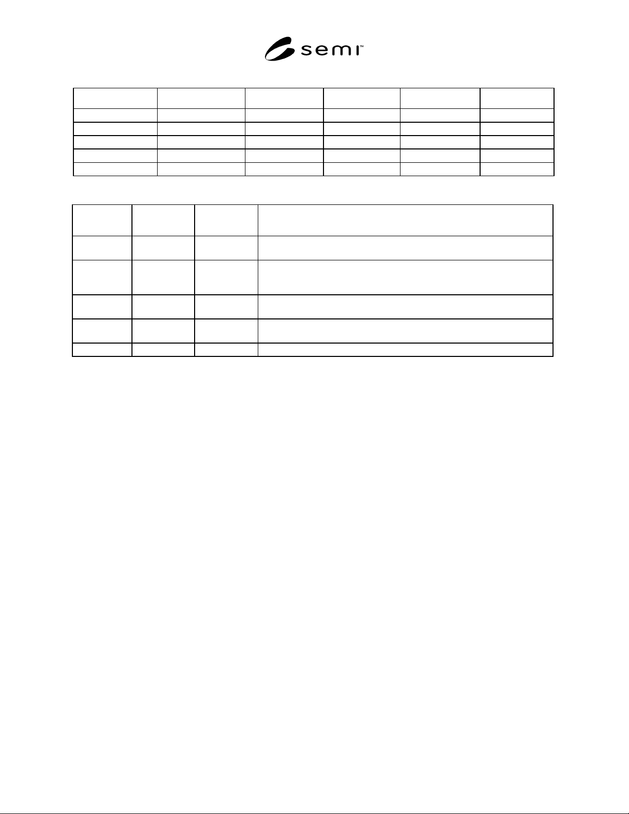
Table 1 Positions for Measurement of Wafer Diameter
Configuration Primary Fiducial Secondary Flat Diameter 1 Diameter 2 Diameter 3
1 270° 180° 45° 135° 165°
2 270° none 0° 45° 135°
3 270° 90° 0° 45° 135°
4 270° 225° 0° 120° 150°
5 270° 135° 0° 30° 60°
Table 2 Wafer Types and Orientations Corresponding to Measurement Configuration of Table 1
Configuration
Conductivity
Type
Orientation Notes
1 p [100] Applies only to [100] p-type wafers, 150 mm and smaller, with secondary
flats
2 p [111] Applies both to [111] p-type wafers, 150 mm and smaller, (without
secondary flats) and to all other notched and flatted wafers without secondary
flats regardless of conductivity type and orientation
3 n [100] Applies only to [100] n-type wafers, 125 mm and smaller, with secondary
flats
4 n [111] Applies only to [111] n-type wafers, 150 mm and smaller, with secondary
flats
5 n [100] Applies only to [100] n-type 150 mm wafers with secondary flats
NOTICE: SEMI makes no warranties or representations as to the suitability of the standards set forth herein for any
particular application. The determination of the suitability of the standard is solely the responsibility of the user.
Users are cautioned to refer to manufacturer' s instructions, product labels, product data sheets, and other relevant
literature, respecting any materials or equipment mentioned herein. These standards are subject to change without
notice.
By publication of this standard, Semiconductor Equipment and Materials International (SEMI) takes no position
respecting the validity of any patent rights or copyrights asserted in connection with any items mentioned in this
standard. Users of this standard are expressly advised that determination of any such patent rights or copyrights, and
the risk of infringement of such rights are entirely their own responsibility.
Copyright by SEMI® (Semiconductor Equipment and Materials
International), 3081 Zanker Road, San Jose, CA 95134. Reproduction o
f
the contents in whole or in part is forbidden without express written
consent of SEMI.