semi合集-English.pdf - 第5266页
SEMI M43-0301 © SE MI 2001 4 RELATED INFORM A TI ON 1 NOT E: T his re lated inform ation is not an of ficial pa rt of SEMI M43 a nd is not inte nded to modif y or supercede the proposed standa rd. It is provided f or inf…
SEMI M43-0301 © SEMI 20013
6.4.3.2 Tabular Representation by % Area Sorted — Specify a threshold T for each D and report the % area.
6.4.3.3 Tabular Representation by Threshold — Specify a % area for each D and report the Threshold, T.
6.4.3.4 Spatial Representation by Height Map — Generate a whole wafer height map of the surface.
6.4.3.5 Spatial Representation by Defect Map — Generate a whole wafer height map of the surface. Analysis areas
whose assigned values (calculated per Section 6.3) exceed the threshold in Section 6.4.3.2 are flagged for each D.
6.4.3.6 Spatial Representation by PV Analysis Map — Generate a whole wafer map of the values assigned in
Section 6.3.
Pixel grid center lines
Center pixel, included
Included pixels
Included pixels, square
D
Pixel grid center lines
Center pixel, included
Included pixels
Included pixels, square
D
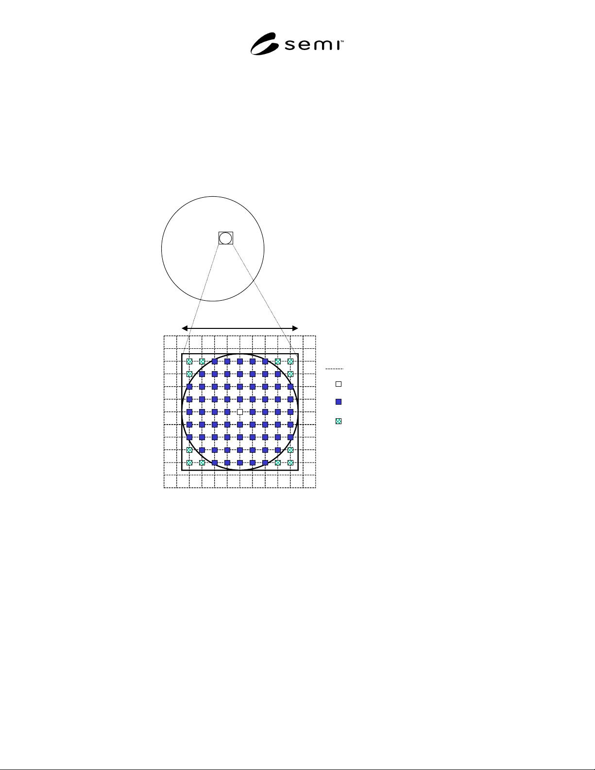
Figure 1
The Analysis Area Of Dimension D, Center And Included Pixels Are Indicated
NOTICE: SEMI makes no warranties or representations as to the suitability of the standard set forth herein for any
particular application. The determination of the suitability of the standard is solely the responsibility of the user.
Users are cautioned to refer to manufacturer’s instructions, product labels, product data sheets, and other relevant
literature respecting any materials or equipment mentioned herein. These standards are subject to change without
notice.
The user’s attention is called to the possibility that compliance with this standard may require use of copyrighted
material or of an invention covered by patent rights. By publication of this standard, SEMI takes no position
respecting the validity of any patent rights or copyrights asserted in connection with any item mentioned in this
standard. Users of this standard are expressly advised that determination of any such patent rights or copyrights, and
the risk of infringement of such rights, are entirely their own responsibility.
SEMI M43-0301 © SEMI 2001 4
RELATED INFORMATION 1
NOTE: This related information is not an official part of SEMI M43 and is not intended to modify or supercede the proposed
standard. It is provided for information purposes. The proposed standard should be referred to in all cases.
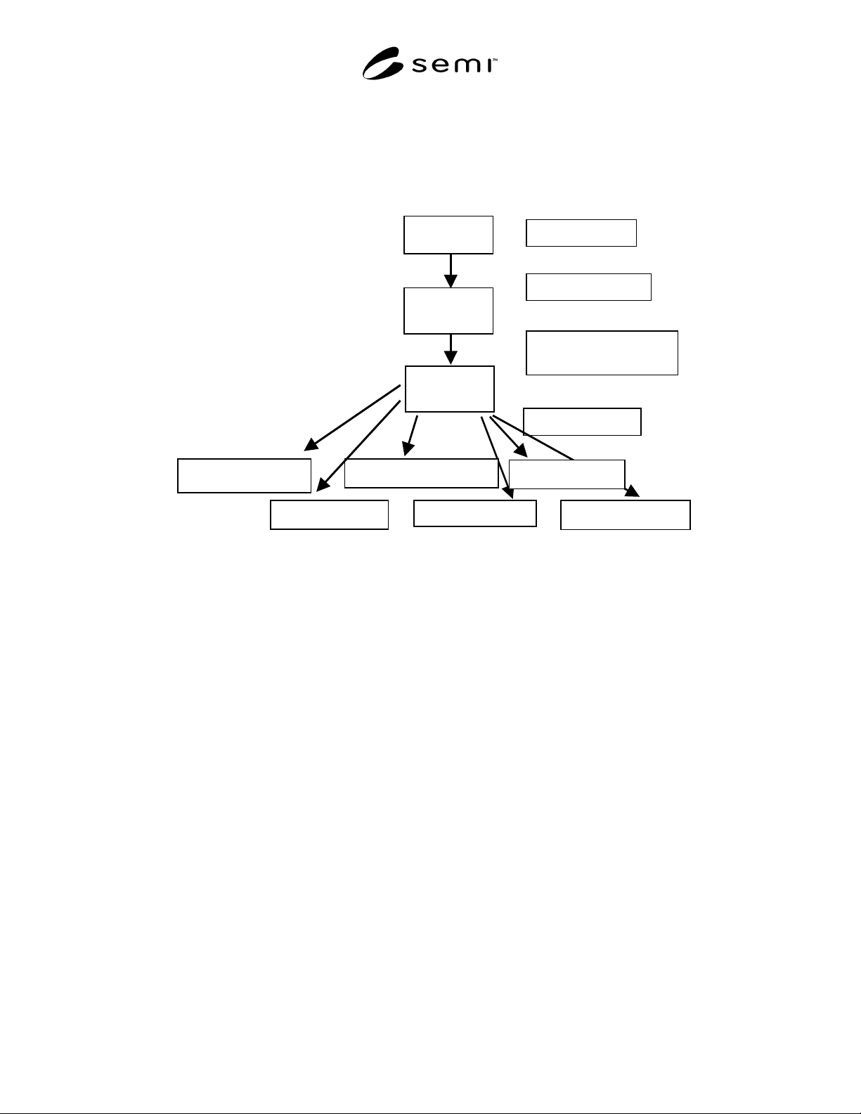
R1-1 SEMI M43 describes reporting wafer nanotopography. The figure below illustrates the flow of data from
measurement through reporting referenced to the document sections.
Height Map
(6.1)
Filtered
Height Map
(6.2)
PV Analysis
Map (6.3)
Threshold Curve (6.4.3.1)
% Area Sorted (6.4.3.2)
Threshold @ % Area (6.4.3.3)
Height Map (6.4.3.4)
Defect Map (6.4.3.5)
PV Analysis Map (6.4.3.6)
1. Acquire Data
2. High Pass Filter
3. Perform Calculation
(for each dimension D)
4. Report Results
Figure R1-1
Nanotopography Reporting Flow
NOTICE: SEMI makes no warranties or representations as to the suitability of the standard set forth herein for any
particular application. The determination of the suitability of the standard is solely the responsibility of the user.
Users are cautioned to refer to manufacturer’s instructions, product labels, product data sheets, and other relevant
literature respecting any materials or equipment mentioned herein. These standards are subject to change without
notice.
The user’s attention is called to the possibility that compliance with this standard may require use of copyrighted
material or of an invention covered by patent rights. By publication of this standard, SEMI takes no position
respecting the validity of any patent rights or copyrights asserted in connection with any item mentioned in this
standard. Users of this standard are expressly advised that determination of any such patent rights or copyrights, and
the risk of infringement of such rights, are entirely their own responsibility.
Copyright by SEMI® (Semiconductor Equipment and Materials
International), 3081 Zanker Road, San Jose, CA 95134. Reproduction o
f
the contents in whole or in part is forbidden without express written
consent of SEMI.

SEMI M44-0305 © SEMI 2001, 2005 1
SEMI M44-0305
GUIDE TO CONVERSION FACTORS FOR INTERSTITIAL OXYGEN IN
SILICON
This guide was technically approved by the Global Silicon Wafer Committee and is the direct responsibility
of the Japanese Silicon Wafer Committee. Current edition approved for publication by the Japan Regional
Standards Committee on January 11, 2005. Initially available at
www.semi.org
January 2005; to be
published March 2005. Originally published March 2001; previously published July 2002.
1 Purpose
1.1 Over the years numerous calibration factors used to calculate the interstitial oxygen content of silicon from the
peak room-temperature infrared absorption at 1107 cm
1
have been standardized by several standards development
organizations in various parts of the world. All such standards have since been revised to use the IOC-88 calibration
factor
1,2
that more correctly relates the true oxygen content of silicon to the absorption peak. Nevertheless, many of
the old calibration factors remain in common use throughout the industry.
1.2 This guide is a compilation of the conversion and calibration factors used in standards established by various
organizations since 1970 for the measurement of interstitial oxygen in silicon.
2 Scope
2.1 This guide allows the user of the guide to convert quantitative values obtained from one standard to another.
2.2 Two tables are included in the guide.
2.2.1 Table 1 gives the calibration factors to relate peak absorption coefficient (cm
–1
) to interstitial oxygen content
in both parts per million atomic (ppma) and atoms/cm
3
for various standards, all of which have been replaced by
newer revisions.
2.2.1.1 These calibration factors are at times referred to by common names as indicated in column 1 of the tables
and at other times by the designation of the (obsolete) standard in which they were standardized (as indicated in the
footnotes to Table 1). Despite the fact that there is a test method associated with each calibration factor, the detailed
procedures in these test methods are usually ignored in common practice and measurements are most frequently
made with automated (black-box) instruments that have internal algorithms. Thus, reference to a particular standard
most often indicates only the value of the calibration factor to be used.
2.2.2 Table 2 gives the conversion factors to convert oxygen concentration of one standard to oxygen concentration
of another standard.
NOTICE: This standard does not purport to address safety issues, if any, associated with its use. It is the
responsibility of the user of this standard to establish appropriate safety and health guides and determine the
applicability of regulatory or other limitations prior to use.
3 Referenced Standards
3.1 SEMI Standards
SEMI M59 — Terminology for Silicon Technology
SEMI MF1188 — Test Method for Interstitial Atomic Oxygen Content of Silicon by Infrared Absorption with Short
Baseline
1 Baghdadi, A., Bullis, W. M., Croarkin, M. C., Li Yue-zhen, Scace, R. I., Series, R. W., Stallhofer, P., and Watanabe, M., “Interlaboratory
Determination of the Calibration Factor for the Measurement of the Interstitial Oxygen Content of Silicon by Infrared Absorption,” J.
Electrochem. Soc. 136, 2015–2034 (1989).
2 Baghdadi, A., Scace, R. I., and Walters, E. J., “Semiconductor Measurement Technology: Database for and Statistical Analysis of the
Interlaboratory Determination of the Calibration Factor for the Measurement of the Interstitial Oxygen Content of Silicon by Infrared
Absorption,” NIST Special Publication 400-82, July 1989.