semi合集-English.pdf - 第4513页
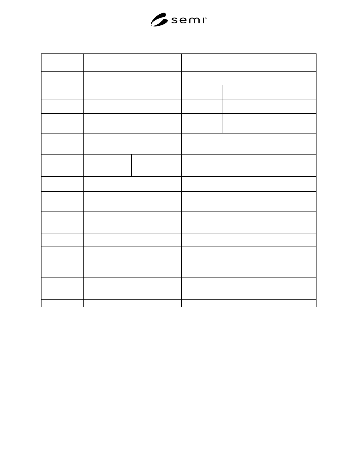
SEMI D24-0200 © SEM I 2000 3 Table 1 Specific ation for Gen III and Larger A ctive-Matrix LCD Substrates Reference Information Range A R ange B Referen ce Documen ts Edge L ength Ranges 550 to 6 50 mm × 650 to 830 mm 750…

SEMI D24-0200 © SEMI 2000 2
6 Test Methods
NOTE 4: The methods described below are approximations,
except where they are followed by a reference such as SEMI
D7. Formal test methods supporting the parameters in this
document will be developed where needed; these will be
published as separate documents. References to them will
then be added to this document.
6.1 Thickness — Measure with differential (2-probe)
gage using optical, non-contact, or contact sensors.
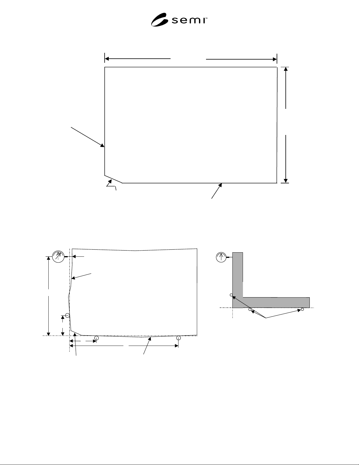
6.2 Edge Squareness — measure p er Figure 2.
6.3 Edge Conditions — to be determined.
6.4 Edge Straightness — measure per Figure 2.
6.5 Total Thickness Variation — to be determined.
6.6 Flatness, medium sheet — to be determined.
6.7 Roughness — SEMI D7 rough ness measurement
method (contact stylus method, tip radium ≤ 2 µm).
6.8 Warp — Feeler gage with thic kness equal to the
specified maximum warp value, inserted between
substrate bottom edge and surface plate, at any point or
at specified points along the edges (formal test
method/description to be developed).
6.9 Waviness — see SEMI D15.
7 Requirements
See Table 1.
8 Ordering Information
8.1 Purchase orders for substrates furnished to this
specification shall include the following items:
8.1.1 Edge length
8.1.1.1 Long reference edge
8.1.1.2 Short reference edge
8.1.2 Orientation corner dimensions , from Table 1
8.1.3 Quality edge area exclusion
8.1.4 Thickness
8.1.4.1 Nominal
8.1.4.2 Tolerance
8.1.5 Warp
8.1.6 Straightness
NOTE 5: Table of Figures:
Figure 1 — Reference Items
Figure 2 — Squareness
Figure 3 — Warp
Figure 4 — Edge Condition
Figure 5 — Orientation and Corner Cuts
Figure 6 — Total Thickness Variation and Local Thickness
Variation
SEMI D24-0200 © SEMI 20003
Table 1 Specification for Gen III and Larger Active-Matrix LCD Substrates
Reference
Information
Range A Range B Reference Documents
Edge Length
Ranges
550 to 650 mm × 650 to 830 mm 750 to1000 mm × 900 to 1100 mm
Edge Length
Dimensions
600 × 720 mm, 650 × 830 mm,
550 × 650 mm
800 × 950 mm 900 × 1100 mm
Edge Length
Tolerance
1
± 0.40 mm ± 0.40 mm ± 0.50 mm SEMI D5 – Std. Sizes
for FPD Substrates
Squareness
1
± 0.83 mm W = ± 0.80 mm
L = ± 0.95 mm
± 1.0 mm SEMI D4 –
Referencing of FPD
Substrates
Edge Condition
9
Rounded
9
Bevel width = 0.1 mm – 0.6 mm, —
extension onto top/bottom surfaces
Rounded
9
Bevel width = 0.1 mm – 0.6 mm
Orientation
Corner
2
1 Corner, Symmetric
C1x = 4.0 ± 1.0 mm
C1y = 4.0 ± 1.0 mm
1 Corner, Asymmetric
C1x = 5.0 ± 1.5 mm
C1y = 2.0 ± 1.5 mm
1 Corner, Asymmetric
C1x = 5.0 ± 1.5 mm
C1y = 2.0 ± 1.5 mm
Corner Cut 3 corners
C2x & C2y = 1.5 ± 1.0 mm
3 corners
C2x & C2y = 1.5 ± 1.0 mm
SEMI D12 – Edge
Condition
Quality Area
3
Edge Exclusion
≤ 10 mm ≤ 20 mm
11
SEMI D3 – Quality
Area for FPD
Substrates
0.7 mm ± 0.07 mm 0.7 mm ± 0.07 mm
SEMI D5 – Std. Sizes
for FPD Substrates
Thickness
1.1 mm ± 0.10 mm 1.1 mm ± 0.10 mm
Total Thickness
Variation
4
60 µm 100 µm
Local Thickness
Variation
5
≤ 20 µm for ≤ 130 mm ≤ 20 µm for ≤ 130 mm
Waviness
6
[W
fpd
]
≤ 0.1 µm, with
λ
C
= 0.8 mm, λ
L
= 8 mm L
S
= 20 mm
≤ 0.1 µm, with
λ
C
= 0.8 mm, λ
L
= 8 mm L
S
= 20 mm
SEMI D15 – Surface
Waviness Measurement
Warp
7
≤ 0.60 mm ≤ 1.0 mm
Roughness, R
a
≤ 20 nm ≤ 20 nm SEMI D7 – Roughness
Measurement
Straightness
8
± 0.4 mm ± 0.4 mm
NOTES:
1 For dimensional tolerance and squareness the long edge typically has the maximum tolerance. See Figures 1 and 2.
2 An asymmetric orientation corner is specified for purposes of mechanical orientation and operator’s visual confirmation of orientation within a
cassette. Optical means of identifying orientation is under investigation. See Figure 5.
3 Quality Area is that area in which the specified criteria apply.
4 Total thickness variation is the peak to valley (TIR) of the entire substrate front surface relative to a reference plane when the substrate back
surface is constrained against a vacuum chuck. This scale is typically important for some film deposition and lithography processes. See Figure
6.
5 Local thickness variation
is the absolute value of the maximum deviation of the substrate from a plane constructed in any 100–130 mm square
area, within the Quality Area, when the substrate back surface is constrained against a vacuum chuck. This scale is typically important for
lithographic stepper processes.
6 Waviness is the rms (root mean square) surface profile, within the quality area, over 0.8–8 mm spatial wavelengths.
7 See Figure 3.
8 See Figure 2.
9 See Figure 4.
10 This table applies to the indicated edge length ranges and thicknesses.
11 Example: For an 800 × 950 mm substrate, the effective process area, which excludes portions not processable for physical reasons, would be ≥
760 × ≥ 910 mm.
SEMI D24-0200 © SEMI 2000 4
(Pattern Surface)
Length (L)
Width (W)
Short Reference
Edge (SRE)
Orientation Corner
Long Reference Edge (LRE)
Figure 1
Reference Items
(Pattern Surface)
Short Reference Edge (SRE)
1 Orientation Corner
Long Reference Edge (LRE)
Dial
Gauge
Pr
a
b
c
d
Calibration using Square
Gauge
Dial
Gauge
Zero
Support pins
NOTE: a, b, c, and d are defined between supplier and customer.
Figure 2
Squareness