semi合集-English.pdf - 第293页
SEMI E47.1-0305 © SEMI 1997, 2005 8 facial datum plane bilateral datum plane y 64 =42.1±0. 5 advancing box sensing pads y 66 50 x 67 34 x 66 31 carrier sensing pads kinemat ic pins info pa d D (FE O L or B E OL ) i…
SEMI E47.1-0305 © SEMI 1997, 2005 7
z
61
15
z
60
=8±0.5
y64 =42.1 ±0.5
z
62
18
y 62
28
y
65
104
facial
datum plane
horizontal datum plane
of load port
y63 =37.3 ±0.5
=30
±0.5°
z63 =7.5
±0.5
r 61
16 (above z 60)
r 60 =16±0.5 (below z 60)
front side of the FOUP
where wafers are accessed
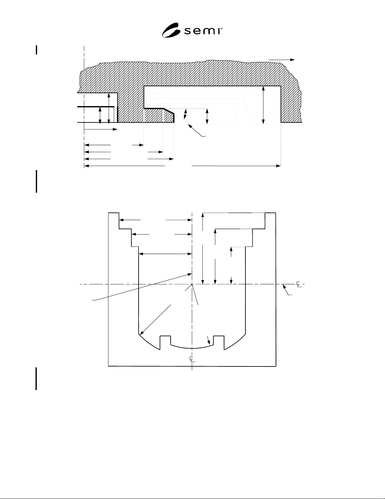
Figure 9
Side View of Retaining Features on Bottom of FOUP
r1
151
(reference
dimension
from SEMI
E1.9)
y52
166
y49
134
y11
85
(from SEMI
E1.9)
x
52
170
facial
datum
plane
x
51
140
x
3
125
(from SEMI E1.9)
bilateral
datum
plane
r4
170 (from
SEMI E1.9)
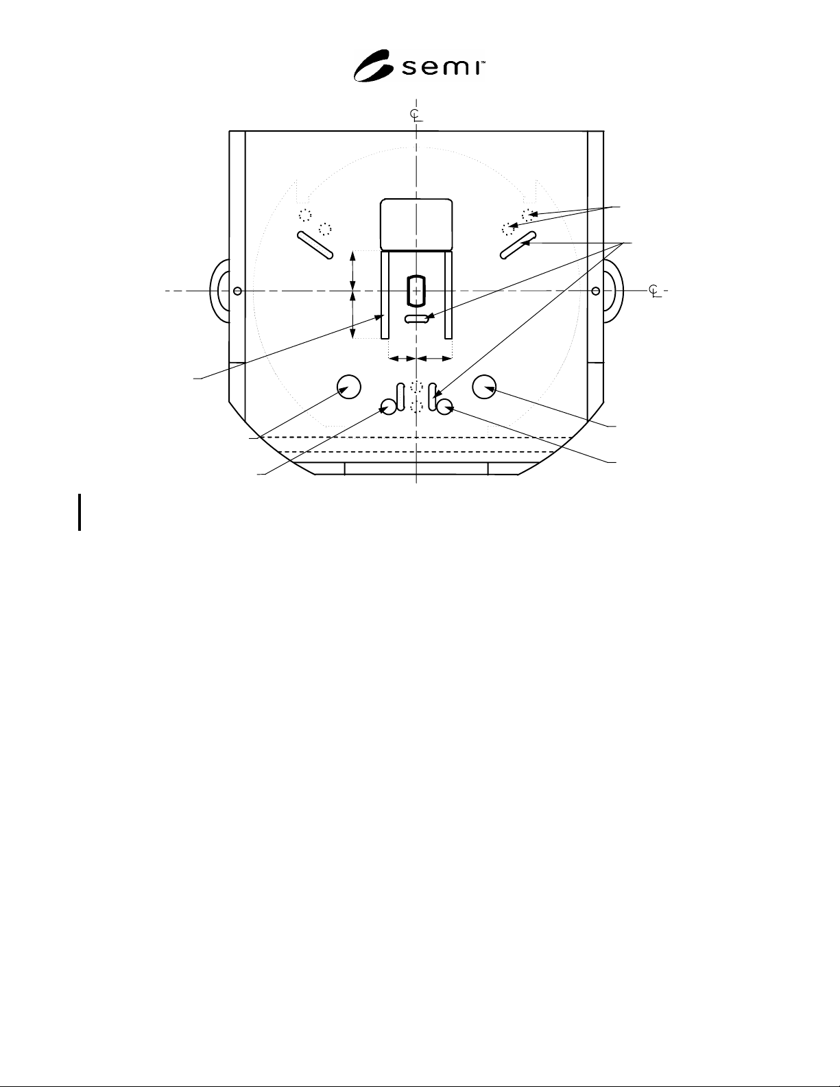
Figure 10
Exclusion Volume Inside FOUP
SEMI E47.1-0305 © SEMI 1997, 2005 8
facial
datum
plane
bilateral
datum
plane
y
64
=42.1±0.5
advancing
box
sensing
pads
y 66
50
x67
34
x66
31
carrier
sensing
pads
kinematic
pins
info pad D
(FEOL or BEOL)
info pad B
(box or cassette)
info pad A
info pad C
Figure 11
Sensing Pads on Bottom of FOUP
SEMI E47.1-0305 © SEMI 1997, 2005 9
x42 =50±1 x41 =30±1
y45
=65.3±1
y47
58
x44 53
facial
datum
plane
bilateral
datum
plane
front side of
the carrier
where wafers
are accessed
y41 =30±1
y46
=71±1
x43 =50±1
x47
58
(16x)
=45
±0.5°
position
notch
orientation
notch
x46 =71±1
x45 =
65.3±1
y44 53
d63
=35±0.1
y68 55
x69 =7.6±0.1
=60°
r63 66
top
of box
bilateral
datum plane
horizontal
datum plane
z
47
=210 (330)
±1
position notch
d
63
=35±0.1
cross-
section
above
x
69 =7.6±0.1
=45±1°
=52±1°
x
45 =65.3±1
x
46 =71±1
z49 8
z
48
15
(numbers in parentheses are for 25-wafer FOUPs, if different)
z
50
5
r
59
6
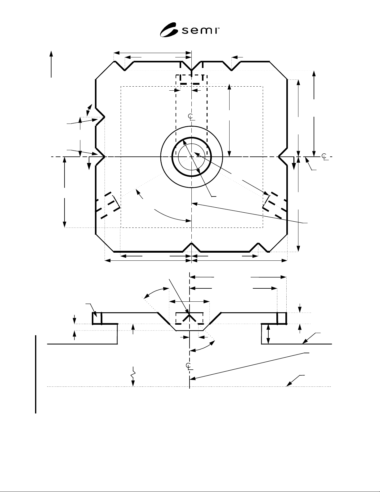
Figure 12
Top Robotic Handling Flange