semi合集-English.pdf - 第6092页
SEMI G16-88 © SEMI 198 3, 1996 3 Figure 2 Figure 3 Figure 4 Shoulder Bend Location VERTICAL, LEAD POSITION Figure 5 Coplanari ty Figure 6 Parting Lin e Protrusion and Variati o n in L ead Locations — Vertical L ead Posit…
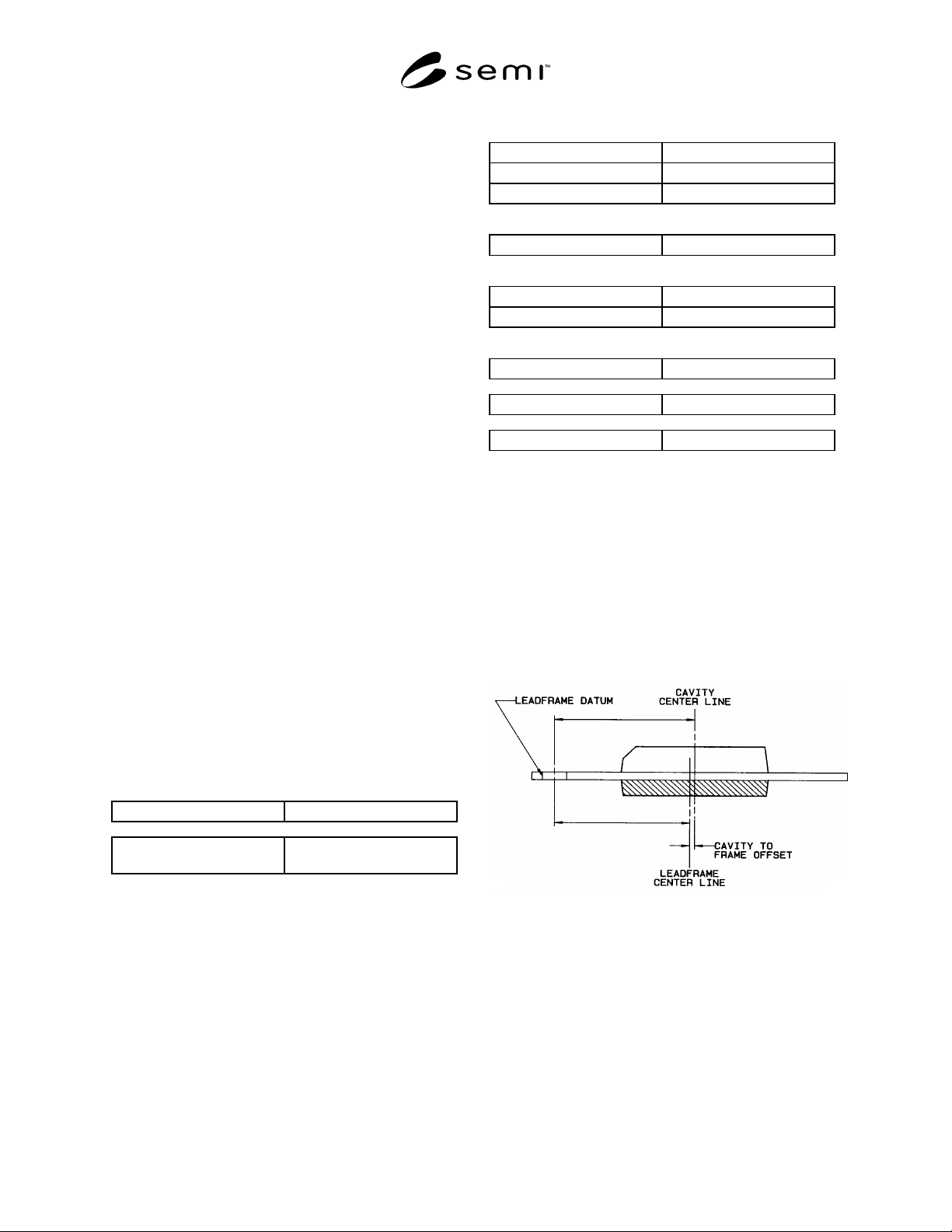
SEMI G16-88 © SEMI 1983, 1996 2
5 Dimensions
5.1 Drawing must show dimensions for the following
items, if applicable:
1. Package length
2. Package width
3. Top cavity thickness
4. Bottom cavity thickness
5. Frame thickness
6. Ejector top locations from cavity center line
7. Ejector bottom locations from cavity center
line
8. Ejector size (top and bottom)
9. Ejector depth (top and bottom, draft angle top
side, bottom side, and end)
10. End notch shape, depth, width, length
11. Pin 1 ID location from package center
12. Pin 1 ID shape and size
13. Corner radius or sides
14. Corner radius or ends
15. Lead spread (nominal)
16. Shoulder bend location
17. Shoulder width
6 Product Criteria Dimensional Tolerance
Limits for PCCs
6.1 In recognizing that every manufacturing process is
subject to variation, the following list details the
acceptable limit of this variation:
CAVITY MISMATCH
0.004" (0.101 mm)
PACKAGE/FRAME
OFFSET
0.002" (0.05 mm) (excluding
leadframe tolerances)
MOLDED PROTRUSIONS
(see Figure 6)
Parting line 0.006" (0.15 mm)
Top or bottom 0.001" (0.025 mm)
VARIATION IN LEAD POSITION
(see Figure 6) 0.004" (0.101 mm)
SHOULDER INTRUSIONS AND PROTRUSIONS
(see Figure 6) Intrusions 0.002" (0.05 mm)
Protrusions 0.003" (0.08 mm)
PACKAGE WARPAGE
Warp factor 2.5
LEAD CO-PLANARITY
0.003" (maximum)
EJECTOR PIN DEPTH
0.010" (maximum)
7 Sampling
7.1 Samples used to determine compliance to Section
6 shall be determined between vendor and supplier.
8 Packaging
8.1 Tooling must be packed in containers designed
and constructed to prevent damage and/or
contamination. Specific protection must be provided if
tooling is to be shipped any great distance.
Figure 1
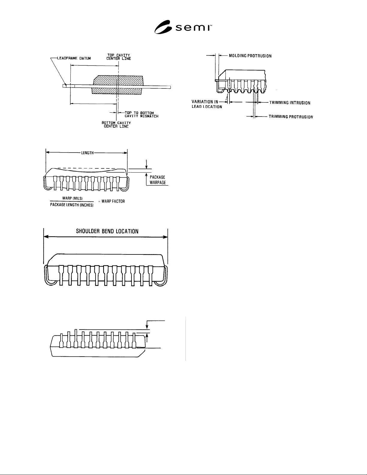
SEMI G16-88 © SEMI 1983, 19963
Figure 2
Figure 3
Figure 4
Shoulder Bend Location
VERTICAL, LEAD POSITION
Figure 5
Coplanarity
Figure 6
Parting Line Protrusion and Variation in Lead
Locations — Vertical Lead Position
NOTICE: These standards do not purport to address
safety issues, if any, associated with their use. It is the
responsibility of the user of these standards to establish
appropriate safety and health practices and determine
the applicability of regulatory limitations prior to use.
SEMI makes no warranties or representations as to the
suitability of the standards set forth herein for any
particular application. The determination of the
suitability of the standard is solely the responsibility of
the user. Users are cautioned to refer to manufacturer’s
instructions, product labels, product data sheets, and
other relevant literature respecting any materials
mentioned herein. These standards are subject to
change without notice.
The user’s attention is called to the possibility that
compliance with this standard may require use of
copyrighted material or of an invention covered by
patent rights. By publication of this standard, SEMI
takes no position respecting the validity of any patent
rights or copyrights asserted in connection with any
item mentioned in this standard. Users of this standard
are expressly advised that determination of any such
patent rights or copyrights, and the risk of infringement
of such rights, are entirely their own responsibility.
Copyright by SEMI® (Semiconductor Equipment and Materials
International), 3081 Zanker Road, San Jose, CA 95134. Reproduction o
f
the contents in whole or in part is forbidden without express written
consent of SEMI.
SEMI G18-96 © SEMI 1984, 19961
SEMI G18-96
STANDARD FOR INTEGRATED CIRCUIT LEADFRAME MATERIAL
USED IN THE PRODUCTION OF ETCHED LEADFRAMES
1 Purpose
This specification is for the leadframe material that will
be shipped to an etch house. It is a leadframe
specification, but deals with material aspects only.
2 Scope
This specification covers the special requirements for
metal strip to be used to fabricate integrated circuit
leadframes by etching.
3 Referenced Documents
3.1 ASTM Specifications
1
ASTM B 601 — Recommended Practice for Temper
Designations for Copper and Copper Alloys —
Wrought and Cast
ASTM E 8 — Methods of Tension Testing of Metallic
Materials
ASTM B 193 — Test Method for Resistivity of
Electrical Conductor Materials
ASTM B 754 — Standard Test Method for Measuring
and Recording the Deviations from Flatness in Copper
and Copper Alloy Strip
4 Terminology
None.
5 Ordering Information
5.1 Orders for material under this specification shall
include the following information:
1. Quantity of each size
2. Alloy name and number
3. Temper or mechanical properties
4. Dimensions: Thickness and width (see Section 7.3.)
5. How furnished: Coils and coil size or sheet size (see
Section 10.)
6. Certification or test report requirements (see Section
11.)
1 American Society for Testing and Materials, 100 Barr Harbor
Drive, West Conshohoken, PA 19428-2959
7. Packaging and marking requirements (see Section
12.)
6 General Requirements
6.1 The materials covered by this specification shall
conform to the requirements detailed in this
specification, unless otherwise agreed upon by supplier
and purchaser.
7 Dimension and Tolerance s
7.1 The following tests shall be used to determine
conformance or non-conformance to this specification.
7.2 Etched Raw Materials Purchased in Coils —
Samples can be taken from the ID or OD of each coil. If
the material does not conform to this specification,
remove two wraps from the ID and OD of each coil and
test for conformance again. Samples may also be taken
from cut sheets.
7.3 Thickness, Width, and Length — The tolerances
for thickness and width shall be as shown in Table 1.
More restrictive tolerances than those shown in Table 1
or tolerances for other thicknesses and widths shall be
agreed upon between user and supplier.
Table 1 Thickness and Width Tolerances
Thickness Tolerance
0.005 - 0.010" (0.127 – 0.254 mm) ± 0.0003" (0.008 mm)
0.015" (0.381 mm) ± 0.0004" (0.010 mm)
0.020" (0.508 mm) ± 0.0005" (0.013 mm)
Width Tolerance
2.000 - 8.000" (25.4 - 203.2 mm) ± 0.005" (0.127 mm)
> 8.000" (> 203.2 mm) to ± 0.010" (0.254 mm)