semi合集-English.pdf - 第6280页
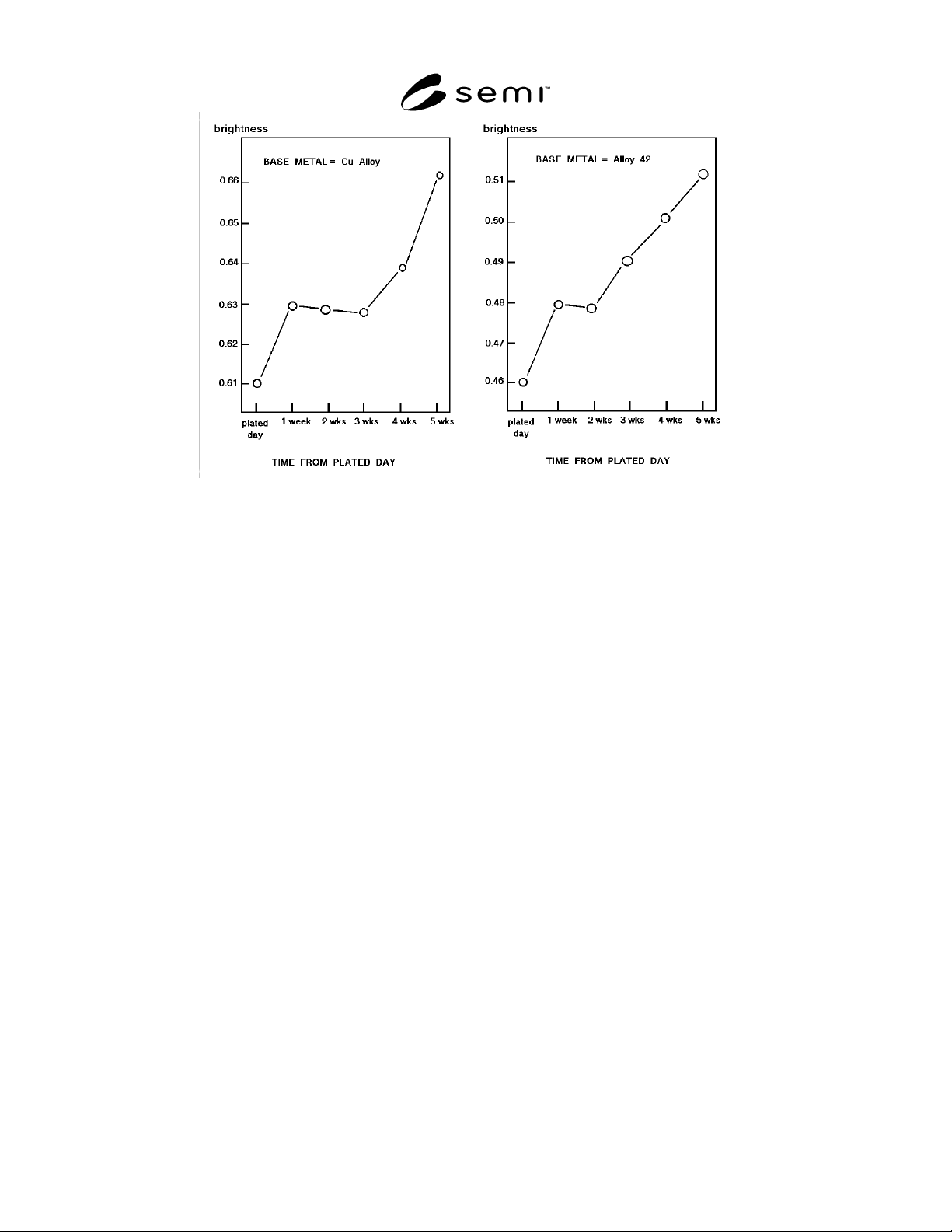
SEMI G55-93 © SEMI 1993, 2004 3 NOTE: Specimens were kept in an office and directly exposed to the atmosphere. Figure 1 Changes of t he Brightness Value as Time Goes by NOTICE: SEMI makes no warranties or represen tation…

SEMI G55-93 © SEMI 1993, 2004 2
an extended time. Results are shown for silver plating
on copper alloy and Alloy 42 leadframes.
6.2.2 Leadframes shall be stored in conditions agreed
between supplier and customer in order to limit
atmospheric tarnishing, and brightness measurements
shall be taken within an agreed time of delivery.
6.3 Degradation of the standards will affect calibration.
7 Equipment
7.1 GAM Densitometer or equivalent.
8 Sampling
8.1 A sampling plan shall be agreed between user and
supplier.
9 Preparation of Samples
9.1 No special preparation requirements are necessary.
Do not contaminate the samples by touching with bare
hands.
10 Measurement Conditions
10.1 To confirm the lamp is on enough to measure the
brightness values. (Lamp intensity is automatically
calibrated.)
11 Equipment Setup and Calibration
11.1 Equipment Setup
11.1.1 Set up and turn on the equipment according to
the manufacturer’s instructions.
11.1.2 Allow at least 30 minutes for equipment
stabilization before beginning measurements.
11.2 Calibration
11.2.1 Calibration shall be performed using standard
black and white plates.
11.2.2 The equipment shall be recalibrated every 30
minutes.
12 Procedure
12.1 Procedure
12.1.1 Measurements shall be made close to the center
of the die pad, if possible. In those situations where the
die pad is not plated, the measurement site shall be
agreed between user and supplier.
12.1.2 Measure all the selected samples according to
the equipment manufacturer’s instructions. Take three
readings on each sample and obtain an average result
for that sample.
12.2 Results
12.2.1 Brightness values shall be rounded to the first
decimal place.
13 Report
13.1 The report, when used by a supplier to certify a
customer’s requirements or by the customer at
incoming inspection shall contain, at least, the
following information, other information which is
reported shall be agreed between supplier and customer.
13.2 Supplier’s Lot Number and Date of Shipment
13.3 Test Conditions
13.4 Results from Section 11. (SPC charting
techniques may be used to monitor results for each
leadframe type and plating requirement.)
14 Repeatability and Precision
14.1 Repeatability
14.1.1 Values for brightness based on use of a
densitometer are repeatable within ± 0.003.
14.2 Precision
14.2.1 Precision for brightness values based on use of a
densitometer is ± 0.015.
SEMI G55-93 © SEMI 1993, 2004 3
NOTE: Specimens were kept in an office and directly exposed to the atmosphere.
Figure 1
Changes of the Brightness Value as Time Goes by
NOTICE: SEMI makes no warranties or representations as to the suitability of the standards set forth herein for any
particular application. The determination of the suitability of the standard is solely the responsibility of the user.
Users are cautioned to refer to manufacturer’s instructions, product labels, product data sheets, and other relevant
literature respecting any materials mentioned herein. These standards are subject to change without notice.
The user’s attention is called to the possibility that compliance with this standard may require use of copyrighted
material or of an invention covered by patent rights. By publication of this standard, SEMI takes no position
respecting the validity of any patent rights or copyrights asserted in connection with any item mentioned in this
standard. Users of this standard are expressly advised that determination of any such patent rights or copyrights, and
the risk of infringement of such rights, are entirely their own responsibility.
Copyright by SEMI® (Semiconductor Equipment and Materials
International), 3081 Zanker Road, San Jose, CA 95134. Reproduction o
f
the contents in whole or in part is for
b
idden without express written
consent of SEMI.

SEMI G56-93 © SEMI 1993, 2002 1
SEMI G56-93 (Reapproved 0302)
TEST METHOD FOR MEASUREMENT OF SILVER PLATING
THICKNESS
This test method was technically approved by the Global Assembly and Packaging Committee and is the
direct responsibility of the Japanese Assembly and Packaging Committee. Current edition approved by the
Japanese Regional Standards Committee on November 26, 2001. Initially available at www.semi.org
December 2001; to be published March 2002. Originally published in 1993.
1 Purpose
1.1 Use — This test may be used for process control
and outgoing inspection at the supplier or by the
customer for incoming inspection.
1.2 Units — This standard test method uses SI units.
2 Scope
2.1 This method describes the standard method for
measuring the thickness of silver plating on
semiconductor leadframes.
2.2 This standard does not purport to address safety
issues, if any, associated with its use. It is the
responsibility of the users of this standard to establish
appropriate safety health practices and determine the
applicability or regulatory limitations prior to use.
3 Referenced Standards
3.1 ASTM Specifications
1
ASTM B 568 — Measurement of Coating Thickness by
X-Ray Spectrometry
4 Significance
4.1 The thickness of plating affects assembly processes
such as wire bonding. If the plating is too thin, heat
processes such as die attach cause the surface to
become unbondable due to bleeding of the base
material through the plating.
4.2 Schematic picture for measurement principles is
shown in Figure 2.
5 Summary of Method
5.1 The method is based on the use of fluorescent X-
rays. This method is chosen as the standard because of
the small measurement area requirements, the high
accuracy of the method for typical silver plating
thicknesses used on leadframes, and the non-contact
method.
1 American Society for Testing and Materials, 100 Barr Harbor
Drive, West Conshohocken, Pennsylvania 19428-2959, USA.
Telephone: 610.832.9585, Fax: 610.832.9555 Website:
www.astm.org
6 Interferences
6.1 Impurities in Plating
6.1.1 Elements with atomic numbers between 42
(Molybdenum) and 52 (Tellurium) cause false readings.
6.2 Measurement Time
6.2.1 At small collimator diameters, the measurement
time is no longer proportional to diameter. X-ray
counting errors may occur for short measurement times.
6.3 Worn or abraded standards will affect calibration.
6.4 Base material variations will affect results.
Standard samples and leadframes must have the same
base material and plating system conditions for accurate
results.
7 Equipment
7.1 Fluorescent X-ray spectrometer.
8 Sampling
8.1 A sampling plan shall be agreed between supplier
and customer.
9 Preparation of Samples
9.1 No special preparation requirements are necessary.
10 Measurement Conditions
10.1 Collimator shall be set at 0.1 mm or 0.3 mm by
agreement between user and supplier.
10.2 Measurement time shall be agreed between user
and supplier.
11 Equipment Setup and Calibration
11.1 Equipment Setup
11.1.1 Set up the equipment according to the
manufacturer’s instructions.
11.1.2 Allow at least 30 minutes for equipment
stabilization before beginning measurements.