semi合集-English.pdf - 第272页
SEMI E45-1101 © SEMI 1995 , 2001 2 3.3 DIN Standards 2 DIN 1265 0 Part 6 — Mechan ical, physical and electrical la boratory apparatus; Piston operated volumetric apparatus; Gravimetric assess ment of metrological reliabi…
SEMI E45-1101 © SEMI 1995, 20011
SEMI E45-1101
TEST METHOD FOR THE DETERMINATION OF INORGANIC
CONTAMINATION FROM MINIENVIRONMENTS USING VAPOR PHASE
DECOMPOSITION-TOTAL REFLECTION X-RAY SPECTROSCOPY
(VPD/TXRF), VPD-ATOMIC ABSORPTION SPECTROSCOPY
(VPD/AAS), OR VPD/INDUCTIVELY COUPLED PLASMA-MASS
SPECTROMETRY (VPD/ICP-MS)
This test method was technically approved by the Global Metrics Committee and is the direct responsibility
of the European Equipment Automation Committee. Current edition approved by the North American
Regional Standards Committee on August 27, 2001. Initially available at www.semi.org September 2001; to
be published November 2001. Originally published in 1995; previously published March 2001.
1 Purpose
1.1 This test method provides the analytical procedures
to determine the level of inorganic contamination from
a minienvironment.
2 Scope
2.1 This document relates to inorganic impurities,
which includes metallic contaminants, whether they
occur as atoms, molecules, or particles. The number of
metals to be analyzed is restricted to the four elements
sodium (Na), calcium (Ca), iron (Fe), and copper (Cu)
in order to rapidly characterize minienvironments from
a practicable point of view. While Na, Ca, and Fe
represent one ensemble of highly detrimental impurities
with respect to contamination from human sources
(Na), the environment (Ca), or from equipment and
corrosive effects (Fe), Cu is analyzed due to its
increasing importance in semiconductor manufacturing.
Additionally, they are easily analyzed with sufficiently
low detection limits. It is up to the user of this test
method to quantify additional elements. A list of
suggested polished wafer surface metal contamination
inappropriate to circuits and devices is shown in Table
1 (based on SEMI M1). The inorganic contamination
on silicon wafer surfaces is collected by VPD.
2.2 To quantify Ca and Fe, VPD/TXRF is used due to
its sufficiently low detection limits. Na and Cu are
quantified by VPD/GFAAS or VPD/ICP-MS. All
analytical methods are widely used for the
characterization of surface cleanliness.
2.3 This measurement technique can also be used to
check the influence of certain process steps on
minienvironments.
2.4 This standard does not purport to address safety
issues, if any, associated with its use. It is the
responsibility of the users of this standard to establish
appropriate safety and health practices and determine
the applicability of regulatory limitations prior to use.
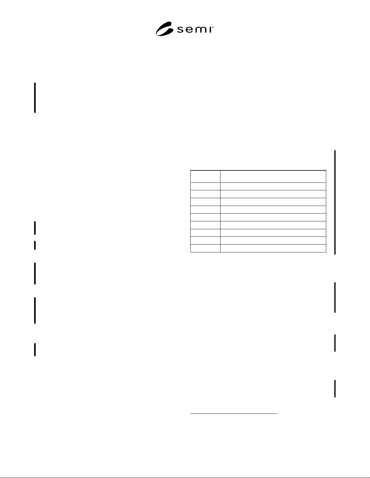
Table 1 Suggested Polished Wafer Surface Metal
Contamination Inappropriate to Circuits and
Devices
Element Test Method
Na VPD/(AAS or ICP-MS)
Al VPD/(AAS or ICP-MS)
K VPD/(AAS or ICP-MS or TXRF)
Cr VPD/(AAS or ICP-MS or TXRF)
Fe VPD/(AAS or ICP-MS or TXRF)
Ni VPD/(AAS or ICP-MS or TXRF)
Cu VPD/(AAS or ICP-MS or TXRF)
Zn VPD/(AAS or ICP-MS or TXRF)
Ca VPD/(AAS or ICP-MS or TXRF)
3 Referenced Standards
3.1 SEMI Standards
SEMI C28 — Specifications and Guidelines for
Hydrofluoric Acid
SEMI C35 — Specifications and Guidelines for Nitric
Acid
SEMI E19 — Standard Mechanical Interface (SMIF)
SEMI M1 — Specification for Polished
Monocrystalline Silicon Wafers
3.2 ISO Standards
1
ISO 9001 — Quality Systems—Model for Quality
Assurance in Design, Development, Production,
Installation, and Servicing
ISO 14644-1 — Cleanrooms and associated
environments – Classification of air cleanliness
1 International Organization for Standardization, ISO Central
Secretariat, 1, rue de Varembé, Case postale 56, CH-1211 Geneva 20,
Switzerland. Website: http://www.iso.ch

SEMI E45-1101 © SEMI 1995, 2001 2
3.3 DIN Standards
2
DIN 12650 Part 6 — Mechanical, physical and
electrical laboratory apparatus; Piston operated
volumetric apparatus; Gravimetric assessment of
metrological reliability
NOTE 1: Unless otherwise indicated, all documents cited
shall be the latest published versions.
4 Terminology
4.1 Abbreviations and Acronyms
4.1.1 GFAAS — Graphite Furnace Atomic Absorption
Spectroscopy
4.1.2 ICP-MS — Inductively Coupled Plasma – Mass
Spectroscopy
4.1.3 PFA — Perfluoroalkoxy
4.1.4 PTFE — Polytetrafluoroethylene
4.1.5 PVDF — Polyvinylidene fluoride
4.1.6 TXRF — Total Reflection X-Ray Fluorescence
Spectroscopy
4.1.7 ULSI — Ultra Large Scale Integration
4.1.8 VPD — Vapor Phase Decomposition
4.2 Definitions
4.2.1 box — a protective portable container for a
cassette and/or substrates.
4.2.2 cassette — an open structure that holds one or
more substrates (e.g., wafer, masks).
4.2.3 DI water — deionized water (specified with
specific resistivity ≥ 18 MΩcm, cations: Na, Cu, Fe, Ca
≤ 0.2 µg/L).
4.2.4 minienvironment — a localized environment
created by an enclosure to isolate the product from
contamination and people.
4.2.5 pod — a box having a Standard Mechanical
Interface (SMIF) (See SEMI E19).
4.2.6 reference wafer — a cleaned wafer (see Section
8.2).
4.2.7 sampling wafer — a cleaned wafer (see Section
8.2), which will be or was exposed to the
minienvironment for a certain time.
4.2.8 standard mechanical interface (SMIF) — the
interface plane between a pod and another
minienvironment (see SEMI E19).
2 Available from Deutches Institut für Normung e.V., Beuth Verlag
GmbH, Burggrafenstrasse 4-10, D-10787 Berlin, Germany. Website:
http://www.din.de
4.2.9 vapor phase decomposition — a method in which
impurities on the surface are collected by the so-called
VPD procedure, i.e., the non-volatile products formed
by acid decomposition of the oxide at the wafer surface
are collected by a droplet of collecting agent, usually
ultra-pure hydrofluoric acid or other reagent or
combination of reagents, and the droplet subsequently
being analyzed by AAS or ICP-MS, or dried in a
manner which gives the least environmental
contamination, the residue from the droplet
subsequently being analyzed by TXRF.
5 Interferences
5.1 For worst cases, preconditioning of wafers can
result in different surface properties indicated by
different sensitivities for contamination absorption.
5.2 Non-linearity effects of the TXRF detector are
significant at higher concentration levels (> 10
13
atoms/cm
2
under the detector area).
5.3 The collection efficiency of VPD depends on:
• the chemistry of the collecting solution
• the bonding of the metal impurities to the silicon
surface
• the speed of the droplet, which is rolled over the
wafer surface
5.3.1 Careful control of contamination and all other
factors affecting the results such as solution
concentrations, scanning methods and other procedures
are necessary to obtain reproducible analytical results.
5.4 The measured TXRF intensity depends on the
accuracy of the procedure to localize and to adjust to
the sampled residue. It also depends on the distribution
of different elements in and around the residue.
5.5 The detection of Fe or Ca using ICP-MS can be
interfered with by background ions originated from the
plasma unless some controlled measures are taken to
minimize these interferences to acceptable levels.
6 Safety Precautions
6.1 Handling hydrofluoric acid is dangerous and shall
be performed according to local regulations for
laboratories. Operators shall be trained to deal with
dangerous chemicals and vapors, especially
hydrofluoric acid and HF vapor. Protective clothes and
glasses must be worn when handling hydrofluoric acid.
7 Apparatus
7.1 The VPD treatment and contamination collection
particularly, but also the handling and measurement of
the specimen wafer is to be carried out in a specified

SEMI E45-1101 © SEMI 1995, 20013
and controlled ambient (e.g., ISO Class 4 (as defined in
ISO 14644-1)).
7.2 The VPD and the advisable drying chamber(s) shall
have opening(s) made of PVDF, PFA, PTFE or similar
resistant and pure polymer materials that are not
attacked by HF. The chamber(s) may contain one or
more wafer stacks. After evacuation, the chamber shall
be flushed with filtered N
2
until the complete drying of
the microdroplet residue is achieved.
7.3 For the aliquots of standard stock and scanning
solutions, validated micropipettes shall be used. DIN
12650 Part 6 provides an applicable validation
procedure.
8 Procedure
These procedures show the determination of Na, Ca,
Cu, and Fe on a silicon wafer surface with
VPD/GFAAS, VPD/ICP-MS and VPD/TXRF. For
achieving best detection limits, VPD/GFAAS and
VPD/ICP-MS shall be used for NA and Cu whereas
VPD/TXRF shall be used for Ca and Fe.
8.1 Test Requirements — The evaluation of the
minienvironment and the analysis shall be carried out
under appropriate clean conditions. Any potential for
cross contamination shall be checked in advance.
Possible contamination sources are:
• VPD preparation
• storage
• contaminated GFAAS or ICP-MS vessels
• environment
• measurement methods and collection efficiency of
VPD
• handling
8.1.1 The capability of the analytical lab has to be
checked carefully for compliance with Sections 8.2,
8.6, and 9.
8.2 Surface Conditions and Cleaning Procedure —
Polished silicon wafers with the following
specifications must be used:
• Specific resistivity = 1–100 Ωcm
• CZ crystal growth method
• Cleaned to leave a native oxide with hydrophilic
surface conditions and with Na, Ca, Cu, and Fe
concentrations lower than 1 × 10
10
atoms/cm
2
8.2.1 Wafer cleaning must be done less than ten
minutes before any further processing. This restricted
time limitation is necessary to ensure cross
contamination avoidance.
8.3 VPD Preparation — The vessel for (opening > 25
cm
2
) inside the VPD box is filled with 25 vol-% HF by
mixing DI water with 50 vol-% VLSI-grade
hydrofluoric acid (see SEMI C28) allowing
hydrofluoric acid of between 25 to 50 wt % to be used.
The wafers are then exposed to the hydrofluoric acid
vapor. Allow wafers exposure to hydrofluoric acid
vapor for 15 to 30 minutes, at which time the wafer
should become hydrophobic due to oxide removal. The
liquid reaction products are collected by rolling a DI
water droplet over the whole wafer surface using up to
100 µL for advisable machine operation or an
appropriate volume for manual operation. Any cross
contamination is minimized by using DI water as
solvent.
8.4 Collection Procedure — An automatic scanning
procedure is preferable, but if the collection procedure
is manual the following procedure should be used.
8.4.1 Use appropriate method to exclude the wafer
edge.
8.4.2 A droplet of collecting agent, usually ultra-pure
hydrofluoric acid or another reagent or a combination
of reagents, is rolled over the whole surface of the
wafer in a parallel pattern.
8.4.3 The same droplet is then moved over the whole
surface, this time in a pattern orthogonal to the first.
8.4.4 Finally, the droplet is rolled in a spiral pattern
from the wafer periphery to its center.
8.5 Pre-analysis Procedure
8.5.1 GFAAS Analysis — The wafer droplet is diluted
to 500 µL.
8.5.2 TXRF Analysis — The droplet is evaporated on
the wafer surface in a clean environment at room
temperature under a nitrogen purge.
8.5.3 ICP-MS Analysis — The wafer droplet is diluted
to 500 µL.
8.6 Sodium and Copper Analysis by GFAAS
8.6.1 Calibration Standards — 1 µg/L for Na.
8.6.2 The calibration frequency and procedures shall be
in accordance with the requirements of the ISO 9001
quality system. The temperature program for the
graphite furnace (dry, ash, atomize) is optimized for
maximum sensitivity. Volatility (e.g., NaF) should be
avoided by spiking the liquid samples with nitric acid
(VLSI grade—see SEMI C35). Prior to analysis of the
liquid sample, a three-point calibration of the element