semi合集-English.pdf - 第7263页
SEMI MF657-0705 © SEMI 2003, 2005 9 NOTICE: SEMI makes no warranties or represen tations as to the suitability o f the standards set forth herein for an y particular application. The determination of the suitability of t…
SEMI MF657-0705 © SEMI 2003, 2005 8
12.2 For referee tests the report shall also include the standard deviation of the warp or TTV (or both) of each wafer
measured, m or (in.).
13 Precision and Bias
13.1 A round-robin experiment was conducted to estimate the precision of this test method.
3
Each of 11
laboratories was to perform three measurements on five 100 mm and five 125 mm diameter polished wafers. The
wafers in each set of five had warp values from about 6 to about 40 m, and TTV values from about 1 to about 5
m.
13.2 Three laboratories used warp measuring equipment that did not conform to the requirements of this test
method, and one additional laboratory did not supply warp data. Two laboratories used TTV measuring equipment
that did not conform to the requirements of this test method. Data from these laboratories were excluded from the
analysis.
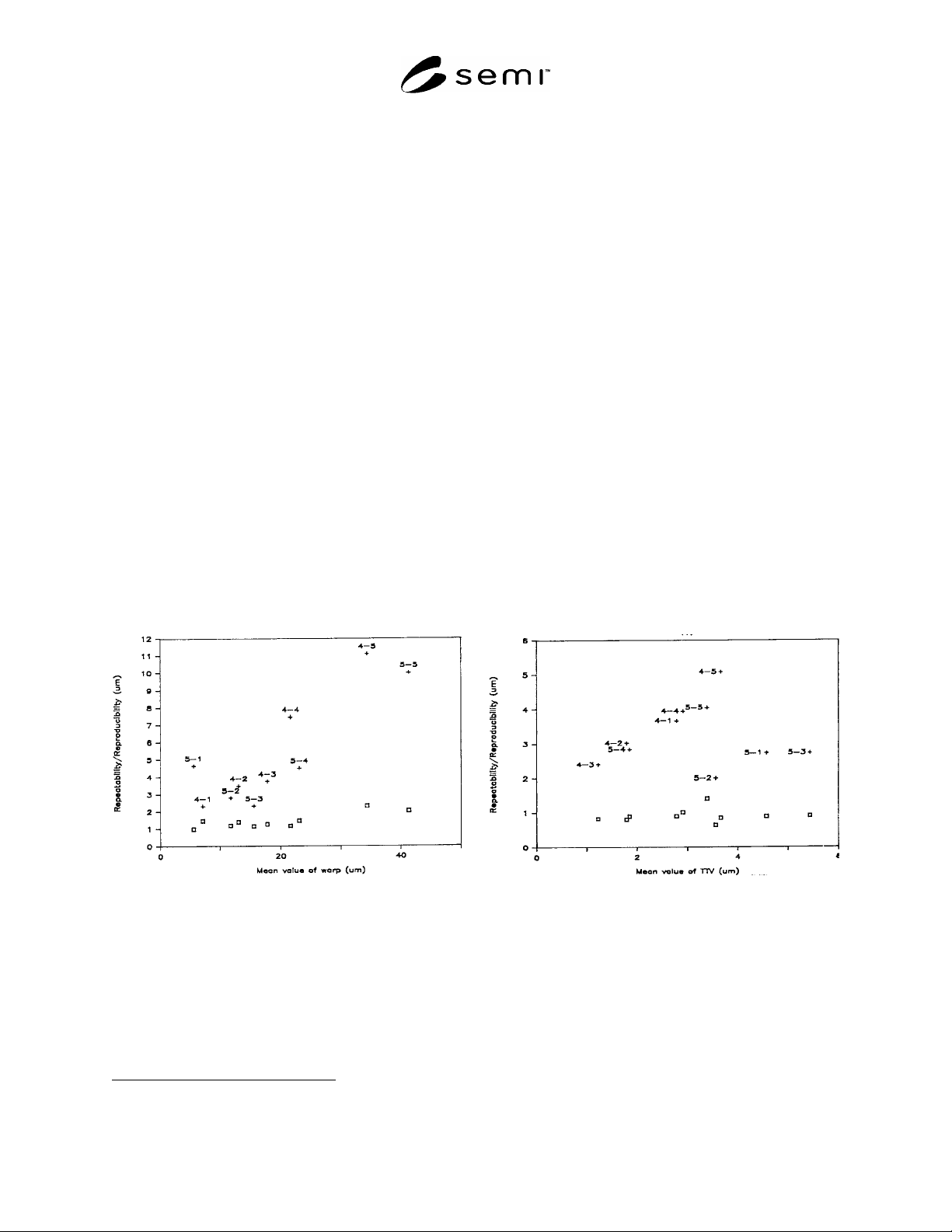
13.3 Based on warp results from seven laboratories and TTV results from nine laboratories, the repeatability (within
laboratory) is estimated to be 1.45 ± 0.42 m and 0.92 ± 0.20 m for warp and TTV, respectively. No significant
difference was noted between measurements on 100 and on 125 mm diameter wafers. There was no significant
trend in repeatability with measured value (see Figure 5).
13.4 The reproducibility (between laboratories) is estimated to be 5.25 ± 3.19 m and 3.25 ± 0.92 m for warp and
TTV, respectively. In this case, there was some increase in the value of warp reproducibility as the warp value
increased and a less pronounced increase in the value of TTV reproducibility as the TTV value increased (see Figure
6).
NOTE 8: In these figures, the numbers are identification numbers. The initial digit represents the approximate nominal diameter
of the sample wafers in inches
13.5 No statement of bias can be made because there are no reference standards against which the result of this
measurement can be compared.
Repeatabilit
y
+
Reproducibility
Repeatabilit
y
+
Reproducibility
Figure 5 Figure 6
Repeatability and Reproducibility of Warp Values Repeatability and Reproducibility of TTV Values
Determined by Interlaboratory Experiment Determined by Interlaboratory Experiment
14 Keywords
14.1 measurement of warp and total thickness variation, (TTV); noncontact scanning; silicon wafers; thickness
variation; warp
3 Supporting data are available on request from SEMI Headquarters, 3081 Zanker Road, San Jose, CA, Telephone 408-943-7021, Fax: 408-943-
7015, e-mail: standards@semi.org. Request International Standards Research Report 1005.

SEMI MF657-0705 © SEMI 2003, 2005 9
NOTICE: SEMI makes no warranties or representations as to the suitability of the standards set forth herein for any
particular application. The determination of the suitability of the standard is solely the responsibility of the user.
Users are cautioned to refer to manufacturer's instructions, product labels, product data sheets, and other relevant
literature, respecting any materials or equipment mentioned herein. These standards are subject to change without
notice.
By publication of this standard, Semiconductor Equipment and Materials International (SEMI) takes no position
respecting the validity of any patent rights or copyrights asserted in connection with any items mentioned in this
standard. Users of this standard are expressly advised that determination of any such patent rights or copyrights, and
the risk of infringement of such rights are entirely their own responsibility.
Copyright by SEMI® (Semiconductor Equipment and Materials
International), 3081 Zanker Road, San Jose, CA 95134. Reproduction of
the contents in whole or in part is forbidden without express written
consent of SEMI.

SEMI MF671-0705 © SEMI 2003, 2005 1
SEMI MF671-0705
TEST METHOD FOR MEASURING FLAT LENGTH ON WAFERS OF
SILICON AND OTHER ELECTRONIC MATERIALS
This test method was technically approved by the global Silicon Wafer Committee. This edition was
approved for publication by the global Audits and Reviews Subcommittee on April 7, 2005. It was available
at www.semi.org in June 2005 and on CD-ROM in July 2005. Original edition published by ASTM
International as ASTM F 671-80. Last previous edition SEMI MF671-99.
1 Purpose
1.1 The length of fiducial flats is an important materials characteristic for determining the suitability of material for
use in semiconductor processing.
1.2 Automatic wafer handling equipment widely used in semiconductor device manufacturing processes relies on
identification and orientation of the primary flat to obtain correct alignment.
1.3 This test method is suitable for use in research, development, process control, quality assurance, and materials
acceptance applications.
2 Scope
2.1 This test method covers techniques for determination of the length of the flatted portion of a wafer periphery.
2.2 This test method is intended primarily for use on electronic materials in the form of nominally circular edge-
contoured wafers with flat lengths up to 65 mm. The precision of this test method has been established directly only
for silicon wafers, but it is not expected to be material dependent.
2.3 This test method is suitable for referee measurement purposes and may be used for routine acceptance
measurements when specified limits require test precision greater than can be obtained with hand held scale and
unaided eye.
2.4 This test method is independent of surface finish.
2.5 For application to wafers of diameter 3 in. or smaller, the values stated in inch-pound units are to be regarded as
the standard whether or not they appear in parentheses; the values stated in acceptable metric units are for
information only. For application to wafers of diameter larger than 3 in., the values stated in acceptable metric units
are to be regarded as the standard; the values stated in inch-pound units are for information only.
NOTE 1: DIN 50441, Part 4, is a similar, but not equivalent method for determining flat length. In this method the flat length is
calculated from a measurement of flat depth. This method does not provide any correction for rounding at the ends of the flat.
NOTICE: This standard does not purport to address safety issues, if any, associated with its use. It is the
responsibility of the user of this standard to establish appropriate safety and health guides and determine the
applicability of regulatory or other limitations prior to use.
3 Limitations
3.1 Some operations performed after slicing, such as mechanical edge grinding and chemical etching, may reduce
profile definition at the ends of the flatted area.
3.2 Backlash in the micrometer head assemblies may result in erroneous readings.
3.3 Failure to maintain sharp focus on the sample comparator screen image during measurement can introduce
errors.
3.4 Comparator optics may sometimes incorporate image-reversal elements, which result in image conditions
opposite to those described by this test method.