semi合集-English.pdf - 第4851页
SEMI M1-0305 © SEMI 1978, 2005 27 Table 6 Dimensional Characteristics of 150 mm Polis hed Monocrystalline Silicon Wafers with Secondary Flat #1 Previous SEMI Reference: SEMI M1.8 Wafer Category: 1.8.1 1.8.2 Property 150 …
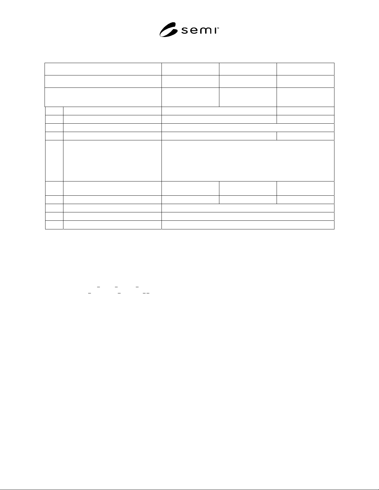
SEMI M1-0305 © SEMI 1978, 2005 26
Table 5 Dimensional Characteristics of 100 mm and 125 mm Polished Monocrystalline Silicon Wafers with
Secondary Flat
#1
Previous SEMI Reference: SEMI M1.5 SEMI M1.6 SEMI M1.7
Wafer Category: 1.5 1.6 1.7
Property
100 mm Wafers
(t=525
m)
#2
100 mm Wafers
(t=625
m)
#2
125 mm Wafers
#2
2-6.1 Diameter
100.00 0.50 mm 125.00 0.50 mm
2-6.2 Primary Flat Length
32.5 2.5 mm 42.5 2.5 mm
2-6.3 Primary Flat Orientation
#3
{110} 1
2-6.4 Secondary Flat Length
18.0 2.0 mm 27.5 2.5 mm
2-6.5 Secondary Flat Location
(See Figure 4)
{111} p-type
{100} p-type
{111} n-type
{100} n-type
No secondary flat
90 5 clockwise from primary flat (
= 180 5)
45 5 clockwise from primary flat (
= 225 5)
180 5 from primary flat (
= 90 5)
2-6.6 Edge Profile Coordinate, C
y
(T/3 Template, see Table 3)
175 m 208 m 208 m
2-6.7 Thickness, Center Point
525 20 m. 625 20 m 625 20 m
2-6.8 Total Thickness Variation, Max.
10 m
2-6.9 Bow, Max.
40 m
2-6.10 Warp, Max.
40 m
#1
Note that these specifications were originated in the United States. Care should be taken in applying this configuration to specific applications
(see ¶6.6.3).
#2
For referee purposes, metric (SI) units apply. To ensure that product shipped is within specification, any conversion to U.S. Customary
equivalents should be done following the maximum-minimum convention in which the minimum values are rounded-up and the maximum values
are rounded-down to ensure that the equivalent range is always inside the referee range. If U.S. Customary equivalents are used for incoming
inspection, minimum values should be rounded-down and maximum values rounded-up to avoid rejection of material that is within the
specification when measured by the referee system of units. CAUTION: The significance of the rightmost digit may vary, depending on the
quantity being measured and the precision of the test procedure. Refer to the relevant test method for precision data which can be used to
construct appropriate guard bands.
#3
For )111( wafers, the
),011( ),101(
, and
)011(
planes are the equivalent, allowable (110) planes. For (100) wafers, the allowable equivalent
)110( planes are
),101( ),011( ),110( and ).110(
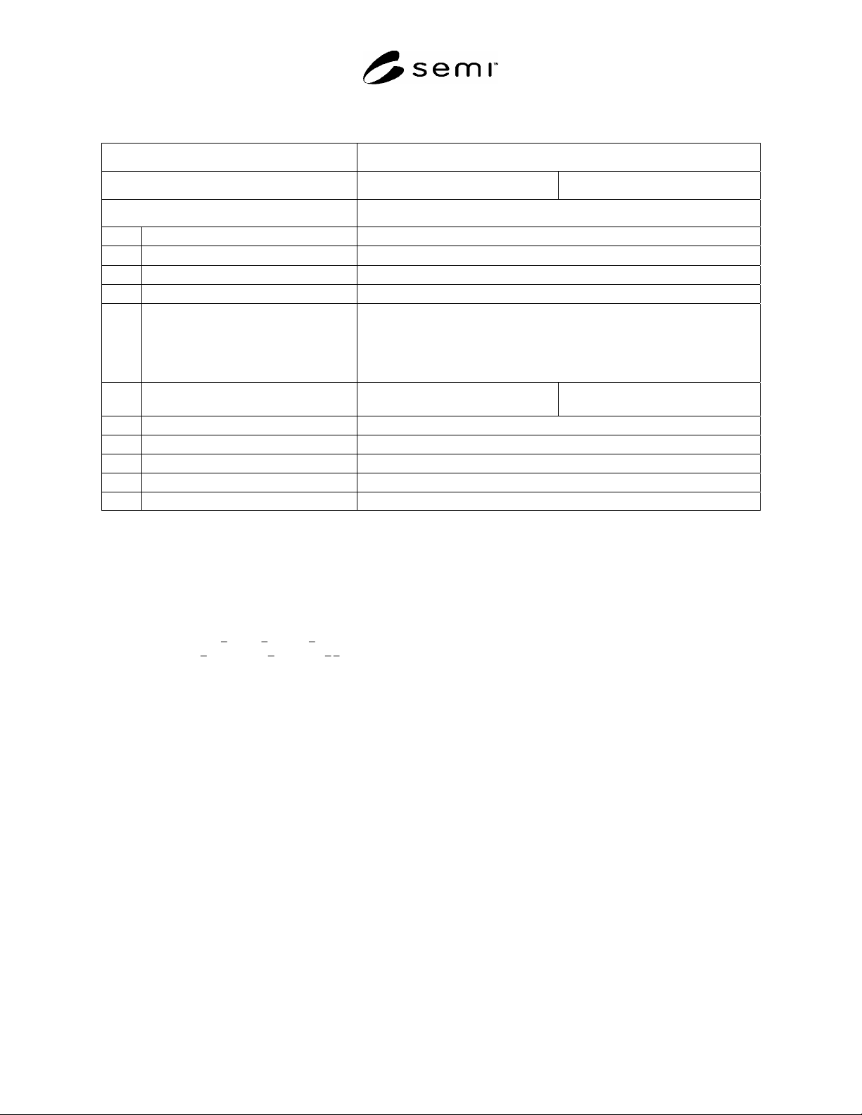
SEMI M1-0305 © SEMI 1978, 2005 27
Table 6 Dimensional Characteristics of 150 mm Polished Monocrystalline Silicon Wafers with Secondary
Flat
#1
Previous SEMI Reference: SEMI M1.8
Wafer Category: 1.8.1 1.8.2
Property 150 mm Wafers
#2
2-6.1 Diameter
150.00 0.20 mm
2-6.2 Primary Flat Length
57.5 2.5 mm
2-6.3 Primary Flat Orientation
#3
{110} 1
2-6.4 Secondary Flat Length
37.5 2.5 mm
2-6.5 Secondary Flat Location (See Figure 4)
{111} p-type
{100} p-type
{111} n-type
{100} n-type
No secondary flat
90 5 clockwise from primary flat (
= 180 5)
45 5 clockwise from primary flat (
= 225 5)
135 5 clockwise from primary flat (
= 135 5)
2-6.6 Edge Profile Coordinate,
C
y
T/3 Template (See Table 3)
225 m
T/4 Template (See Table 3)
169 m
2-6.7 Thickness, Center Point
675 20 m
2-6.8 Total Thickness Variation, Max.
10 m
2-6.9 Bow, Max.
60 m
2-6.10 Warp, Max.
60 m
2-5.7 Edge Surface Condition Supplier-customer agreement
#4
#1
Note that these specifications were originated in the United States. Care should be taken in applying this configuration to specific applications
(see ¶6.6.3).
#2
For referee purposes, metric (SI) units apply. To ensure that product shipped is within specification, any conversion to U.S. Customary
equivalents should be done following the maximum-minimum convention in which the minimum values are rounded-up and the maximum values
are rounded-down to ensure that the equivalent range is always inside the referee range. If U.S. Customary equivalents are used for incoming
inspection, minimum values should be rounded-down and maximum values rounded-up to avoid rejection of material that is within the
specification when measured by the referee system of units. CAUTION: The significance of the rightmost digit may vary, depending on the
quantity being measured and the precision of the test procedure. Refer to the relevant test method for precision data which can be used to
construct appropriate guard bands.
#3
For )111( wafers, the
),011( ),101( , and )011( planes are the equivalent, allowable (110) planes. For (100) wafers, the allowable equivalent
)110( planes are
),101( ),011( ),110( and ).110(
#4
If specified as polished, this term is meant to imply a surface condition and not a particular processing technique. If desired, a quantitative
measure of surface finish may optionally be indicated by specifying the rms microroughness over a specified spatial frequency (or wavelength)
range. Because a standardized test method has not yet been developed for this metric, both values and test procedures, including sampling plan
and detrending procedures, shall be agreed upon between supplier and customer.
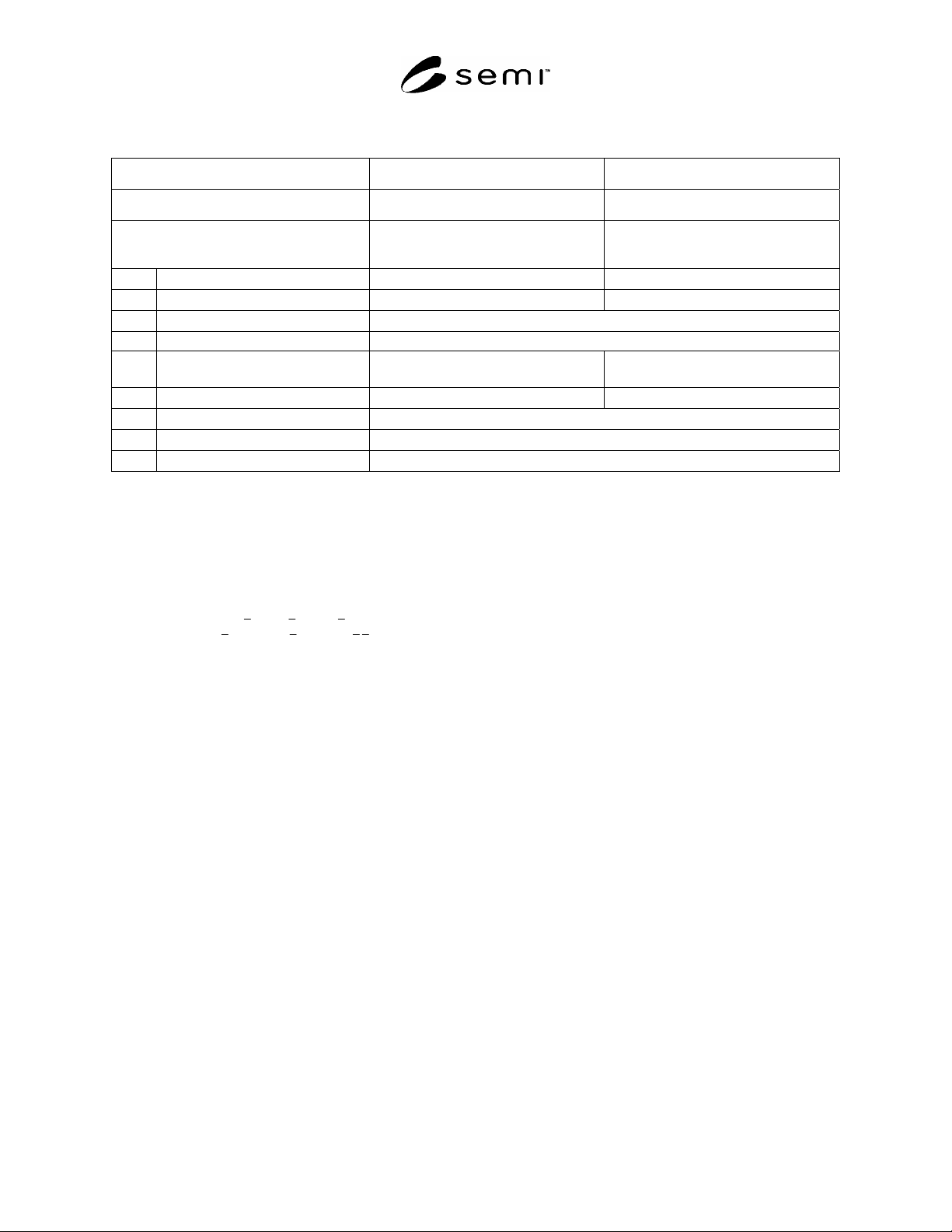
SEMI M1-0305 © SEMI 1978, 2005 28
Table 7 Dimensional Characteristics of 100 mm and 125 mm Polished Monocrystalline Silicon Wafers
without Secondary Flat
#1
Previous SEMI Reference: SEMI M1.11 SEMI M1.12
Wafer Category: 1.11 1.12
Property
100 mm Wafers without secondary flat
(t=525
m)
#2
125 mm Wafers without secondary flat
(t=625
m)
#2
2-6.1 Diameter
100.00 0.20 mm. 125.00 0.20 mm
2-6.2 Primary Flat Length
32.5 2.5 mm 42.5 2.5 mm
2-6.3 Primary Flat Orientation
#3
{110} 1
2-6.5 Secondary Flat Location No secondary flat
2-6.6 Edge Profile Coordinate, C
y
(T/3 Template, see Table 3)
175 m 208 m
2-6.7 Thickness, Center Point
525 15 m. 625 15 m
2-6.8 Total Thickness Variation, Max.
10 m
2-6.9 Bow, Max.
40 m
2-6.10 Warp, Max.
40 m
#1
Note that these specifications were originated in Japan. They are equivalent to the specifications for wafers of the same nominal diameter in
JEITA EM-3602. Care should be taken in applying this configuration to specific applications (see ¶6.6.3).
#2
For referee purposes, metric (SI) units apply. To ensure that product shipped is within specification, any conversion to U.S. Customary
equivalents should be done following the maximum-minimum convention in which the minimum values are rounded-up and the maximum values
are rounded-down to ensure that the equivalent range is always inside the referee range. If U.S. Customary equivalents are used for incoming
inspection, minimum values should be rounded-down and maximum values rounded-up to avoid rejection of material that is within the
specification when measured by the referee system of units. CAUTION: The significance of the rightmost digit may vary, depending on the
quantity being measured and the precision of the test procedure. Refer to the relevant test method for precision data which can be used to
construct appropriate guard bands.
#3
For )111( wafers, the
),011( ),101(
and
)011(
planes are the equivalent, allowable (110) planes. For (100) wafers, the allowable equivalent
)110( planes are
),101(),011( ),110( and ).110(