semi合集-English.pdf - 第5213页
SEMI M38-1104 © SEMI 1999, 2004 12 RELATED INFORMATION 1 BACKGROUND INFORMATION FOR MU LTIPLE LASER MARKING (RE- INSCRIPTION) OF 300 mm POLISHED SILICON RECL AIMED WAFERS NOTICE: This related information is not an offici…
SEMI M38-1104 © SEMI 1999, 2004 11
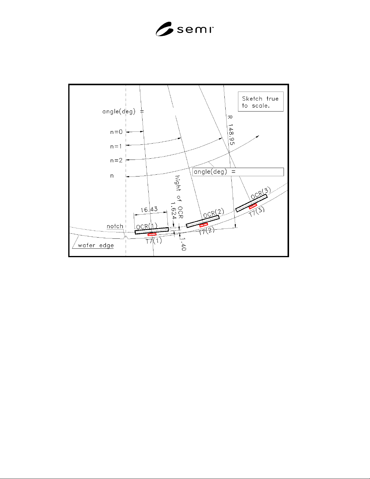
A1-5.2 Maintaining Inscription Utility — The angle of the new inscription shall be provided to the customer by the
supplier so that the tool used to read the inscriptions can be adjusted to read the wafer ID at the new angle. Since it
is possible for a tool to be provided the wrong angle to read an inscription, as long as the information remains the
same as the prior inscription, errors can be minimized (read attempts at different angles).
5° + n × 10°
5°
15°
25°
5° + n × 10°
Figure A1-1
Locations of Original Inscription and Subsequent Re-inscriptions on Back Surface of
Notched 300 mm Diameter Reclaimed Wafer

SEMI M38-1104 © SEMI 1999, 2004 12
RELATED INFORMATION 1
BACKGROUND INFORMATION FOR MULTIPLE LASER MARKING (RE-
INSCRIPTION) OF 300 mm POLISHED SILICON RECLAIMED WAFERS
NOTICE: This related information is not an official part of SEMI M38. It was developed by the International 300
mm Reclaim Remark Task Force during the development of the specification for multiple-laser marking of 300 mm
polished silicon reclaimed wafers. This related information was approved for publication by full letter ballot
procedures on August 16, 2004.
R1-1 Multiple Laser Making Issues
R1-1.1 Issues related to multiple laser marking of 300
mm silicon reclaimed wafers were explored at meetings
during SEMICON West in San Francisco in July 2002,
SEMICON Southwest in Austin in October 2002,
SEMICON Japan in Tokyo in December 2002 and a ½
day workshop during SEMICON Europa in Munich in
April 2003. Significant input from device makers,
wafer reclaimers, and equipment suppliers was
received.
R1-1.2 Four major issues emerged.
R1-2 When Is a Remark
Field Applied?
R1-2.1 This could be at each reclaim cycle, or when
the “first” mark is not readable at the reclaimer.
R1-2.2 Because the latter is a difficult matter, it was
decided to make this a decision of the purchaser.
R1-3 Where Should the Remark Field(s) Be
Located?
R1-3.1 A device manufacturer suggested that each new
remark field be located 10 counter clockwise (CCW)
from the previous mark field, and at the same radius.
R1-3.2 A wafer with two of more fields is
unambiguously identified as a reclaim wafer and the
“n” remarked fields it contains indicate the number of
reclaim cycles it has experienced, if it is remarked after
each use.
R1-4 What Is the Remark Field’s Content?
R1-4.1 Two scenarios are possible:
R1-4.1.1 Different from the Original Mark — For
example, retaining the ID # but changing the supplier
code from original to the reclaim supplier’s code. This
could confuse a device fab’s database when two
identical ID numbers appear in the database unless it
also includes the vendor code. Changing the ID
number does not necessarily avoid this problem.
R1-4.1.2 Same as the Original Mark — This simplifies
the remark coding. However, the is still the possibility
of confusing the device manufacturer’s database.
R1-4.2 It was decided to make this a decision of the
purchaser.
R1-5 How to “Disable” a Previous Mark Field?
R1-5.1 Disabling a mark field requires that a mark
field be modified or obliterated sufficiently to ensure
the reader reports a “no read.”
R1-5.2 It was decided to make both the requirement to
obliterate the previous mark and the method of
obliteration decisions of the purchaser.
R1-6 Mark Field Obliteration Comments.
R1-6.1 Obliterating an entire field may not be
necessary to make it unreadable. For the two mark
fields specified in SEMI M1.15, the following may
apply:
R1-6.1.1 Data Matrix Field
R1-6.1.1.1 Reliable reading of this field requires a
quiet zone (no surface disturbance) about four dots
wide (400 µm) around the field periphery. Filling the
quiet zone with dots insures that the Data Matrix mark
cannot be read.
R1-6.1.1.1.1 Surrounding the 8 row 32 column field
with a 4-dot border involves (8 + 32) 2 4 = 320
dots.
R1-6.1.1.1.2 A 3-dot border may work as well, and
requires 240 dots.
R1-6.1.1.2
Conversely, overwriting the field involves
8 32 = 306 dots.
R1-6.1.1.2.1 A difference of 100 µm (one dot) between
the positions of the overwrite field and original field
should still produce a “no read.”
R1-6.1.1.2.2 Some position difference results from the
marker’s wafer alignment system. The alignment
capability of deployed 300 mm markers is therefore a
consideration.
R1-6.2 Alphanumeric Field
R1-6.2.1 Obliterating one or more message characters
and one or more check sum characters should make the
mark unreadable by both camera and human readers.

SEMI M38-1104 © SEMI 1999, 2004 13
This requires completely overwriting each of these
characters with a filled 5 × 9 character field (45 dots at
“single density”). It was suggested this be done at two
ID characters (1 and 6 in the 12-character string) and
one check sum character (12).
R1-6.2.2 This overwriting involves 3 fields 45 dots =
135 dots.
R1-6.2.3 The alignment comments in Section R1-
6.1.1.2.2 also apply to these fields.
R1-7 Use of Remarked Reclaimed Wafers in
Device Fabrication
R1-7.1 This may involve two scenarios:
R1-7.1.1 Incoming Search
R1-7.1.2 Determine the “good” remark field location
(5 + [10 n]) degrees from the notch bisector for each
wafer and store that data in the factory database. Then
the manufacturing execution system commands a tool
handling that wafer to go to the appropriate field
location. This minimizes or eliminates throughput
effects.
NOTE 1: This requires variable read location capability (by
wafer rotation, for instance) on the tool.
R1-7.2 Local Tool Search
R1-7.2.1 When unable to read the original field, the
tool scans counterclockwise until it finds a readable
field. This cycle can adversely impact tool throughput.
NOTE 2: This requires
Variable read location capability and
“Smart” read, i.e., 3 levels, as follows:
Good read (this is the “right” field, so keep the
data),
Bad read (this is an obliterated field, go to
“next” location and try again), and
No read (no mark is present, search somewhere
else).
NOTICE: SEMI makes no warranties or
representations as to the suitability of the standards set
forth herein for any particular application. The
determination of the suitability of the standard is solely
the responsibility of the user. Users are cautioned to
refer to manufacturer's instructions, product labels,
product data sheets, and other relevant literature,
respecting any materials or equipment mentioned
herein. These standards are subject to change without
notice.
By publication of this standard, Semiconductor
Equipment and Materials International (SEMI) takes no
position respecting the validity of any patent rights or
copyrights asserted in connection with any items
mentioned in this standard. Users of this standard are
expressly advised that determination of any such patent
rights or copyrights, and the risk of infringement of
such rights are entirely their own responsibility.
Copyright by SEMI® (Semiconductor Equipment and Materials
International), 3081 Zanker Road, San Jose, CA 95134. Reproduction of
the contents in whole or in part is forbidden without express written
consent of SEMI.