semi合集-English.pdf - 第5440页
SEMI M60-0305 © SEMI 2005 8 proper identification of the failure criteria. It is possibl e that ra pid voltage c h anges at the dielectric breakdown of the gate oxide cause electrical noise. Th ere is a possibility that …
SEMI M60-0305 © SEMI 2005 7
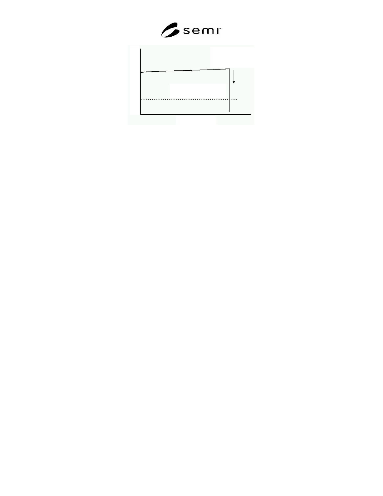
Drop of applied
gate voltage at
breakdown
Breakdown judgement
voltage level
Applied Gate Voltage (V)
Time (sec)
Drop of applied
gate voltage at
breakdown
Breakdown judgement
voltage level
Applied Gate Voltage (V)
Time (sec)
NOTE: A typical applied gate voltage as a function of stress time and a relationship between a drop of the applied gate voltage at
dielectric break-down and breakdown judgment voltage level.
Figure 2
6 Significance and Use
6.1 This standard gives the procedure for characterizing mirror-polished, p-type CZ silicon wafers using the
dielectric breakdown defect densities of the gate oxide thermally grown on them. The MOS capacitors shall be
formed in accordance with the fabrication processes described in §5 and SEMI M51. This reason is because the
oxide characteristics depend on the fabrication processes. If MOS capacitors would be formed with different
fabrication processes, it is desirable to confirm that these GOI results are similar to those of the MOS capacitors
formed by the fabrication processes described above. Particularly, the electrode material of the MOS capacitors has
a great influence on the dielectric breakdown of the gate oxide. Poly-silicon is specified as the electrode material in
this standard. The test with the poly-silicon gate electrode gives us the test results directly applicable to the wafers
for the integrated circuits rather than other metal electrodes, because poly-silicon electrodes are commonly used in
actual devices. Of course other materials are also available for electrodes. Where other electrode material is used,
an appropriate method for each case and the correlation data between poly-silicon and the other material shall be
prepared.
6.2 It is well known that both the silicon surface morphology and the cross-sectional structure at the pattern edge of
the active region of the MOS devices influence the dielectric breakdown of the gate oxide. Various types of
contaminants also influence the dielectric breakdown of the gate oxide. The extent of contamination by alkaline
metals, heavy metals or organic particles increases, as the sample fabrication process progresses.
6.2.1 The electrode area and total number of MOS capacitors shall be chosen to be suitable for the purpose of the
test. The suitable gate area for the constant current TDDB measurement depends on the applied stress (i.e. induced
current). If the gate electrode area is too large, parasitic resistance of the gate electrode disturbs uniform application
of stress current to gate oxide. That is, too a high current density leads to nonuniform stress on gate oxide. As a
result, the reliability of the measurement is reduced. The gate oxide with a defect density is able to be evaluated
using two sets of MOS capacitors. Although the gate area and total number of MOS capacitors have the same
product, one set consists of many capacitors with a small gate area and the other set consists of a few of capacitors
with a large gate area. The TDDB evaluations using the former are more desirable than those using the latter. In
this round robin, where a polycrystalline silicon thickness is 300 nm, sheet resistance is 50/ and gate area is
smaller than 5 mm
2
, reasonable TDDB results were obtained.
7 Interferences
7.1 Since this is a DC measurement, care must be taken to make sure that the silicon wafer has a low-resistance
ohmic contact. There must be no dielectric film on the back surface, e.g., silicon oxide, in order to effectively apply
a voltage bias to the gate oxide. It is not necessary for this to be carried out with a metallic contact on the back
surface of the wafer under test. However, when the vacuum chucking is weak, care must be taken because of the
possibility that the dielectric breakdown of the gate oxide is not accurately judged due to an increase in parasitic
resistance. It is strongly suggested that testing be carried out with a current polarity such that the silicon surface will
be in accumulation below the gate oxide, that is, negative voltages for p-type silicon wafers. If the polarity of the
voltage is chosen to be in the reverse direction, the breakdown voltage may not be accurately measured due to the
presence of a depletion layer below the gate oxide. Controls of electrical noise in this test method are crucial to the

SEMI M60-0305 © SEMI 2005 8
proper identification of the failure criteria. It is possible that rapid voltage changes at the dielectric breakdown of
the gate oxide cause electrical noise. There is a possibility that this noise leads to misjudgments of the oxide
breakdown. So it is desirable to confirm that oxide breakdown occurred. For example after the TDDB
measurement has been completed, the samples are measured to confirm their insulation. Mechanical stress due to
the exploring probe can influence the measurement results, because the exploring probe is in contact with the gate
electrode directly on the gate oxide. The actual results obtained depend somewhat on the sample fabrication
process. Care must be taken to ensure consistent processing. Wafer temperature during testing shall be clearly
defined. Large temperature variations might have an impact on results.
7.1.1 Precaution — Since the voltages and currents involved are potentially dangerous, appropriate means of
preventing the operator from coming into contact with the exploring probe or other charge surfaces shall be in place
before testing. This standard does not include any clauses relating to the safety and sanitation of the environment.
Those who intend to implement this standard shall consider appropriate means to prevent any accidents or disasters,
as well as taking responsibility for maintaining a state of safety, health and hygiene for users.
8 Sampling
8.1 Sampling is the responsibility of the user of this test method. However, if testing is carried out as part of a
comparison or a correlation, all participants shall agree upon sampling in advance.
NOTE 3: Refer to the appendix of JEDEC standard No.35 for good discussion of sampling plan statistics.
9 Apparatus
9.1 SEMI M51 and SEMI M1771 shall be applied for measurement equipment such as current/voltage source units
and manual probing machines
10 Procedure
10.1 Fabrication of MOS Capacitors
10.1.1 Refer to SEMI M51, introducing poly-silicon as an electrode material. Where another electrode material is
used, an appropriate method for each case and the correlation data between poly-silicon and the other material shall
be prepared.
10.2 Measurement
10.2.1 Before measurement, record the following information for each sample: date, time, operator, sample ID,
oxide thickness, gate area, gate material, oxidation condition, conductivity type (p or n), equipment ID, and
comments.
10.2.2 Decide on measurement parameters and record them. Constant current is applied in this test method. The
parameters include stress current density (J), measurement interval (T
int
), maximum stress time (T
max
), gate area (S),
judgment voltage of breakdown (V
bd
), measurement temperature, the number of capacitors to be measured and a
map of the capacitors.
10.2.3 Set a tungsten exploring probe at the starting position.
10.2.4 Set the exploring probe on a new MOS capacitor at the next position.
10.2.5 Set the accumulated time to zero (T (0) = 0). Record the oxide leakage current and the voltage.
10.2.6 Set the stress current to the designated point. Monitor the time (t) and the voltage (V
t
) from the start.
10.2.7 If the applied time is equal to or greater than the maximum stress time(t T
max
), record the maximum stress
time (T
max
) as the breakdown time (T
bd
) along with the MOS address, and proceed to ¶10.2.8. If t is less than T
max
,
proceed to the next step.
10.2.8 Check to see if the voltage Vt has reached the judgment voltage of breakdown (V
bd
). If so, record the time
(t), along with each MOS address, as the breakdown time (T
bd
), stop applying the stress current, and proceed to
¶10.2.9. If not, repeat from ¶10.2.6.

SEMI M60-0305 © SEMI 2005 9
10.2.9 Check to see if there are any more MOS capacitors to be measured. If so, repeat from ¶10.2.4 until all MOS
capacitors have been tested. A contact probe for all measuring points eliminates the need for repeat of the
measurement, and proceeds to the next wafer.
10.2.10 Report the results.
10.2.11 Figure 3 shows a flow diagram outlining the procedure for this test method.
10.2.12 For the judgment method of breakdown, not only fixed V
bd
but variation in voltage (V) monitored could
be used.
10.2.13 Figure 4 shows a flow diagram outlining the procedure for the test method when the judgment of
breakdown by drop in voltage (V) is adopted.