semi合集-English.pdf - 第6059页
SEMI G8-94 © SEMI 1 983, 199 6 3 10.4 Funct ional Tests 10.4.1 Die Att ach and W ire Bond 10.4.1.1 Die A ttac h and Wire Bond tes t s shall be performed using m aterial s and conditions agreed between v e ndor and cu sto…

SEMI G8-94 © SEMI 1983, 1996 2
5.4 pitting (plated metal layer) — Unspecified
depressions in the plated layer, not the underlying
layer(s). Such pits may be caused by incorrect plating
conditions.
5.5 resin bleed-out (die attach) — The surface creep of
a resin used for die attach beyond the outer perimeter of
the bulk of the resin (filler). For a given resin
formulation, the resin creep may be exacerbated by the
microstructure and cleanliness of the die attach surface.
5.6 scratch — An abrasion in the surface of a
metallization layer which exposes the base material.
6 Interferences
6.1 Avoid contaminating the gold plated surface (e.g.,
with finger oils), prior to performing the tests. Such
contamination may effect visual appearance, and die
attach, wire bond, and solderability functional tests.
7 Equipment
7.1 Beta Backscatter system
7.2 Die Attach equipment
7.3 Eutectic Die Attach heater block or lot plate
capable of 450 °C ± 10 °C.
7.4 Microscope 10-30× magnification with vertical
lighting.
7.5 Micro Cross-Section equipment
7.6 Wire Bond equipment
7.7 X-Ray Fluorescence System
8 Sampling
8.1 Sampling plans shall be agreed between vendor
and customer.
9 Test Sequence
When the test methods are used at incoming inspection
the sequence of test shall be as follows:
9.1 Visual Appearance — See Section 10.1.
9.2 Plating Thickness — See Section 10.2.
9.3 Plating Adhesion — See Section 10.3.
9.4 Functional Tests (Die Attach, Wire Bond, and
Lead Solderability) — See Section 10.4.
9.5 Salt Atmosphere Test — See Section 10.5.
9.6 Plating Hardness — See Section 10.6.
10 Test Procedures
10.1 Visual Inspection
10.1.1 Components shall be visually inspected
according to the appropriate component specification
for plating requirements.
10.1.2 Surface Structure — The gold plate shall be
smooth matte to semi-bright in appearance. Minor
variations in color are not cause for failure at this stage
unless there is evidence of corrosion, peeling, or pitting
in the plating layer.
Note 2: For the purposes of this test method, particular
attention shall be observed in relation to blisters and adhesion
problems with the plating layer.
10.2 Plating Thickness
10.2.1 Plating thickness shall be measured at locations
agreed upon between vendor and customer.
10.2.2 Plating thickness may be measured by one of
the following techniques, which are listed in order of
preference.
ASTM Method B 568
ASTM Method B 567
ASTM Method B 487
Note 3: Method B 487 shall only be used for thicknesses
greater than 100 microinches (0.0025 mm).
10.3 Plating Adhesion
10.3.1 Submit samples to 450 °C ± 10°C for two (2)
minutes in air on a die attach heater block or hot plate.
10.3.2 Visually inspect the plating under the
microscope set at 10× magnification for blistering,
peeling, and discoloration.
Note 4: Discoloration after the heat testing is only allowable if
the gold plate thickness is less than 20 micro-inches (508
micro mm) by design. Amount and type of discoloration shall
be agreed upon between vendor and customer.
Note 5: 30×
magnification may be used for confirmation.
10.3.3 Adhesion Tape Test — Flat Surface
10.3.3.1 Place a strip of tape across the plated area.
Press firmly with finger tips or another smooth object.
10.3.3.2 Peel the tape quickly off the plated surface. If
there is any plating on the tape the component shall be
rejected.
10.3.4 Lead Finish Adherence — Bend Test
10.3.4.1 Bend the leads once through a 90° angle on a
diameter equal to the lead diameter or thickness.
10.3.4.2 Visually inspect the plating under the
microscope set at 10× magnification for evidence
peeling or cracking of the plated layer.

SEMI G8-94 © SEMI 1983, 19963
10.4 Functional Tests
10.4.1 Die Attach and Wire Bond
10.4.1.1 Die Attach and Wire Bond tests shall be
performed using materials and conditions agreed
between vendor and customer.
10.4.1.2 Die Attach shall be evaluated for shear
strength per MIL-STD-883, Method 2019 or by a
method agreed between vendor and customer.
Resin bleed-out shall also be evaluated when the extent
of the bleed may affect subsequent wire bonding
processes.
10.4.2 Solderability
10.4.2.1 Solderability testing, with or without aging,
shall be agreed between vendor and customer.
Solderability testing shall be performed per MIL-STD-
883, Method 2003.
10.5 Salt Atmosphere Test
10.5.1 Salt Atmosphere Testing Requirements —
Applicability and condition shall be agreed between
vendor and customer. Salt atmosphere testing shall be
performed per MIL-STD-883, Method 1009 or MIL-
STD-750, Method 1041 as appropriate.
10.6 Plating Hardness
10.6.1 If specified, the plating hardness shall be
determined by one of the following methods as
appropriate:
ASTM B 384
ASTM E 10
Note 6: Hardness testing for thin plating is difficult and not
very reliable. The hardness specification shall be agreed
between user and supplier.
NOTICE: These standards do not purport to address
safety issues, if any, associated with their use. It is the
responsibility of the user of these standards to establish
appropriate safety and health practices and determine
the applicability of regulatory limitations prior to use.
SEMI makes no warranties or representations as to the
suitability of the standards set forth herein for any
particular application. The determination of the
suitability of the standard is solely the responsibility of
the user. Users are cautioned to refer to manufacturer’s
instructions, product labels, product data sheets, and
other relevant literature respecting any materials
mentioned herein. These standards are subject to
change without notice.
The user’s attention is called to the possibility that
compliance with this standard may require use of
copyrighted material or of an invention covered by
patent rights. By publication of this standard, SEMI
takes no position respecting the validity of any patent
rights or copyrights asserted in connection with any
item mentioned in this standard. Users of this standard
are expressly advised that determination of any such
patent rights or copyrights, and the risk of infringement
of such rights, are entirely their own responsibility.
Copyright by SEMI® (Semiconductor Equipment and Materials
International), 3081 Zanker Road, San Jose, CA 95134. Reproduction o
f
the contents in whole or in part is forbidden without express written
consent of SEMI.
SEMI G9-89 © SEMI 1980, 19961
SEMI G9-89
SPECIFICATION FOR STAMPED LEADFRAMES FOR PLASTIC
MOLDED DUAL-IN-LINE SEMICONDUCTOR PACKAGES
1 Preface
This specification is a guideline for the stamping
manufacture of leadframes for plastic molded dual-in-
line semiconductor packages. It is a design guideline
for packaging engineers, leadframe stampers and mold
manufacturers, and has been developed to meet the
requirements of automatic bonding.
2 Applicable Documents
2.1 This document specifically ref ers to:
SEMI G4 — Specification for Integrated Circuit
Leadframe Materials Used in the Production of
Stamped Leadframes
SEMI G10 — Standard Method of Mechanical
Measurement
SEMI G21 — Specification for Plating Integrated
Circuit Leadframes
2.2 Related information may also be found in:
MIL-STD-105
1
— Sampling Procedures and Tables for
Inspection by Attributes
MIL-STD-883 — Test Methods and Procedures for
Microelectronics
3 Selected Definitions
burr — A fragment of excess material either horizontal
or vertical attached to the leadframe.
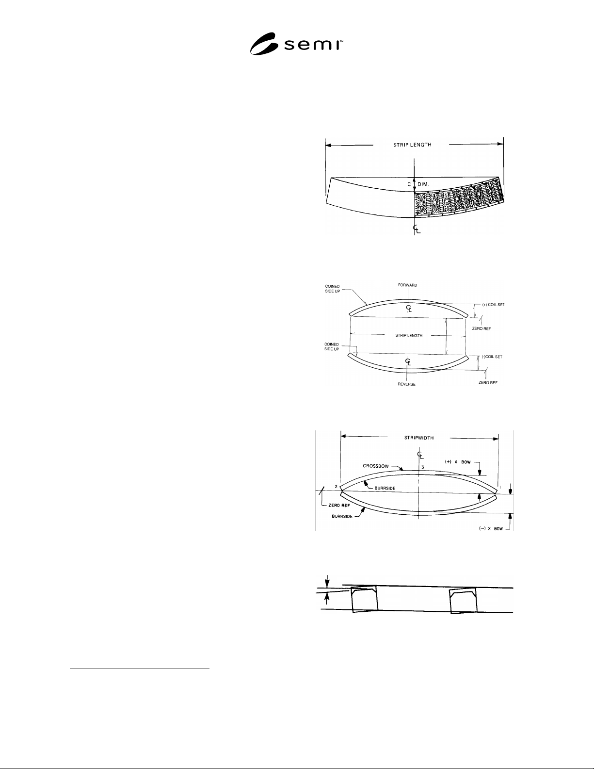
camber — Curvature of the leadframe strip edge (see
Figure 1).
coil set — Longitudinal bowing of the leadframe strip
length (see Figure 2).
coined area — Reference lead flat surface.
crossbow — Transverse bowing of the leadframe (see
Figure 3.)
functional area — The die attach pad and the lead tips.
lead flat surface — Area on the lead tips that is suitable
and available for wire bonding. This is generally
achieved by coining on stamped leadframes and is also
known as the coined area on such leadframes.
1 Military Standards, Naval Publications and Form Center, 508 Tabor
Ave., Philadelphia, PA 19120
Figure 1
Camber
Figure 2
Coil Set
Figure 3
Crossbow
Figure 4
Lead Twist