semi合集-English.pdf - 第7868页
SEMI T13-1104 © SEMI 2004 28 List 2 An Example of D evice ID Data in XML <? xml version ="1.0" encoding ="utf-8" ?> < DeviceIdData xmlns ="urn:semi-org:xsd.Doc3754.V0312.DeviceIdData&quo…
SEMI T13-1104 © SEMI 2004 27
List 1 An Example of Device Tracking Data in XML
<?xml version="1.0" encoding="utf-8" ?>
<
DeviceTrackingData xmlns="urn:semi-org:xsd.Doc3754.V0312.DeviceTrackingData">
<SubstrateType>Strip</SubstrateType>
<SubstrateId>MyStrip</SubstrateId>
<LayoutId>Device</LayoutId>
<OriginLocation>LowerLeftTop</OriginLocation>
<RowColumnMajor>Column</RowColumnMajor>
<FromSubstrate>
<SubstrateType>Wafer</SubstrateType>
<SubstrateId>Wafer1</SubstrateId>
<D><X>10</X><Y>18</Y></D>
<D><X>7</
X><Y>17</Y></D>
</FromSubstrate>
<FromSubstrate>
<SubstrateType>Wafer</SubstrateType>
<SubstrateId>Wafer2</SubstrateId>
<D><X>18</X><Y>1</Y></D>
<D><X>9</X><Y>0</Y></D>
</FromSubstrate>
</
DeviceTrackingData>
NOTE 1: The <D> elements contain the X and Y location on the substrate from which they came.
NOTE 2: The <FromSubstrate> element specifies the substrate type and identifier from which the devices came from.
NOTE 3: The <D> elements represent each device on the layout “Device” for strip “MyStrip”.
NOTE 4: The number of <D> entries must equal Rows * Columns defined in the “Device” layout.
NOTE 5: The one dimensional array of <D> elements represents the two dimensional array of locations defined in the “Devices” layout in
RowColumnMajor format with respect to the OriginLocation.
NOTE 6: The OriginLocation corresponds to the definition of the same name in SEMI G81.
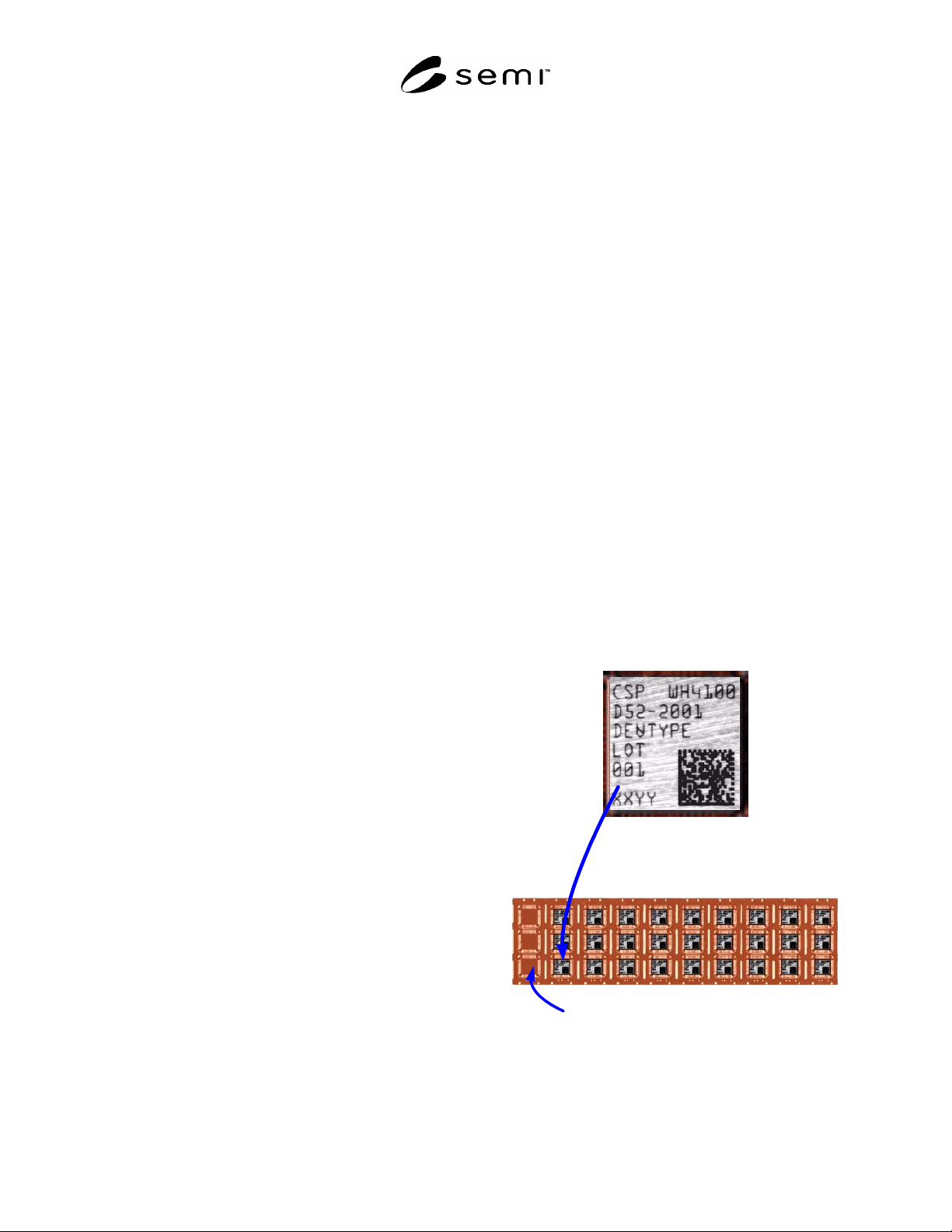
R1-2 Device ID Report
R1-2.1 ID Example — The following figure shows a
strip of devices with alphanumeric and 2D matrix
marks. The unique part of the 2D mark is “LOT001-
XXYY”.
R1-2.2 Report Example — The following list shows a
truncated version of the Device Id Data report for the
strip shown in upper figure.
Substrate
Index = 3
Rows = 3
Columns = 10
ToX = 1
ToY = 1
OriginLocation (0,0) ="LowerLeftTop"
RowColumnMajor="Column"
DeviceId
Figure R1-2
SEMI T13-1104 © SEMI 2004 28
List 2 An Example of Device ID Data in XML
<?xml version="1.0" encoding="utf-8" ?>
<
DeviceIdData xmlns="urn:semi-org:xsd.Doc3754.V0312.DeviceIdData">
<SubstrateType>Strip</SubstrateType>
<SubstrateId>MyStrip</SubstrateId>
<LayoutId>Device</LayoutId>
<OriginLocation>LowerLeftTop</OriginLocation>
<RowColumnMajor>Column</RowColumnMajor>
<D><Id></Id></D>
<D><Id></Id></D>
<D><Id></Id></D>
<D><Id>Lot001-XXYY</Id></D>
<D><
Id>etc.</Id></D>
</
DeviceIdData>
NOTE 1:The <D> elements contain a tracking code marked on the package that is unique for the manufacturer and product.
NOTE 2: The <D> elements represent each device on the layout “Device” for strip “MyStrip”.
NOTE 3: The number of <D> entries must equal Rows * Columns defined in the “Device” layout.
NOTE 4: The one dimensional array of <D> elements represents the two dimensional array of locations defined in the “Devices” layout in
RowColumnMajor format with respect to the OriginLocation.
NOTE 5: The OriginLocation corresponds to the definition of the same name in SEMI G81.
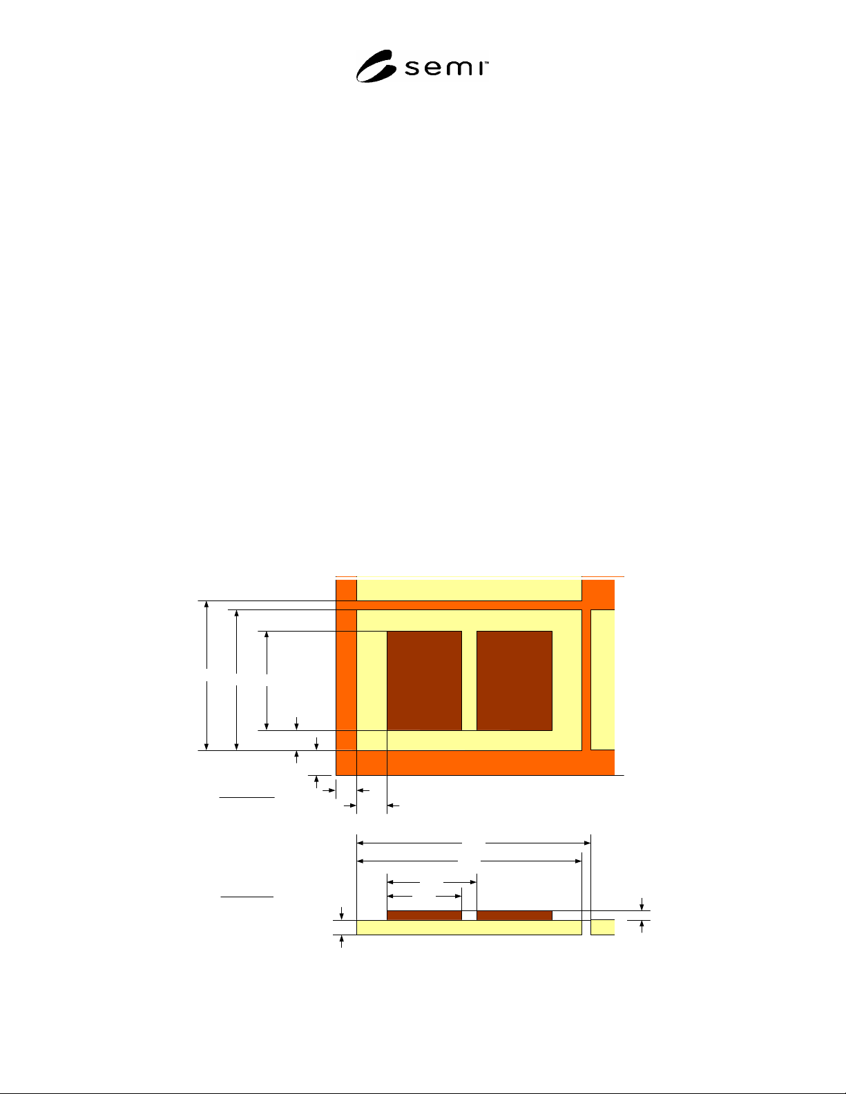
R1-3 Substrate Layout Data Report
R1-3.1 Substrate Layout Example — The following figure shows the lower left corner of a strip that contains an
array of SRAM devices with 2 Flash devices mounted on each.
R1-3.2 Layout Representation Example — The following list shows the substrate layout data that represents the
strip shown in the figure.
SRAM
FlashFlash
30.00
75.00
78.00
33.00
46.67
49.67
5.00
3.00
SRAM Layout
Dimension (X=32, Y=8)
LowerLeft (X=7.00, Y=8.33)
StepSize (X=78.00, Y=49.67)
DeviceSize (X=75.00, Y=46.67)
Height = 5.00
ZOrder = 0
25.00
7.00
8.33
Flash Layout
Dimension (X=2, Y=1)
LowerLeft (X=10.00, Y=6.67)
StepSize (X=30.00, Y=0.00)
DeviceSize (X=25.00, Y=33.0)
Height = 3.00
ZOrder = 1
6.67
10.00
Figure R1-3

SEMI T13-1104 © SEMI 2004 29
List 3 An Example of Substrate Layout Data in XML
<?xml version="1.0" encoding="utf-8" ?>
<
SubstrateLayoutData xmlns="urn:semi-
org:xsd.Doc3754.V0312.SubstrateLayoutData">
<SubstrateType>Strip</SubstrateType>
<SubstrateId>MyStrip</SubstrateId>
<LayoutId>Device</LayoutId>
<Units>100micron</Units>
<Size><X>2510.00</X><Y>414.02</Y></Size>
<Layout>
<LayoutId>SRAM</LayoutId>
<Dimension><X>32</X><Y>8</Y></Dimension>
<LowerLeft><X>
7.00</X><Y>8.33</Y></LowerLeft>
<StepSize><X>78.00</X><Y>49.67</Y></StepSize>
<DeviceSize><X>75.00</X><Y>46.67</Y></DeviceSize>
<Z><Order>0</Order><Height>5.00</Height></Z>
<Layout>
<LayoutId>FLASH</LayoutId>
<Dimension><X>2</X><Y>1</Y></Dimension>
<LowerLeft><X
>10.00</X><Y>6.67</Y></LowerLeft>
<StepSize><X>30.00</X><Y>0.00</Y></StepSize>
<DeviceSize><X>25.00</X><Y>33.00</Y></DeviceSize>
<Z><Order>1</Order><Height>3.00</Height></Z>
</Layout>
</Layout>
</
SubstrateLayoutData>