semi合集-English.pdf - 第4893页
SEMI M4-1103 © SEMI 1978, 2003 3 Figure 1 Measurement Points for Determination of Layer Thickness Variation 7.2.3 Resistivity — Determi n e by a method agreed upon betwee n supplie r and purc haser. Contacting method: SE…

SEMI M4-1103 © SEMI 1978, 2003 2
4.1.5 lot — for the purpose of this document, (a) all of
the wafers of nominally identical specification and
characteristics contained in a single shipment, or (b)
subdivisions of large shipments consisting of epitaxial
wafers as above which have been identified by the
supplier as constituting a lot.
4.1.6 pre-epitaxial treatment — the process of etching
an amount of material from the sapphire substrate in
situ prior to deposition.
NOTE 2: Hydrogen (H
2
) gas is commonly used for this
purpose.
4.1.7 resistivity (Ω·cm) — for the purpose of this
method, the volume resistivity, the ratio of the potential
gradient parallel to the current in the material to the
current density.
4.1.8 silicon source — volatile or gaseous silicon
compound.
NOTE 3: Silane (SiH
4
) gas is commonly used for this
purpose.
4.1.9 substrate — the polished sapphire slice upon
which the epitaxial layer is deposited.
4.1.10 surface defects — refers to mechanical
imperfections, SiO
2
residual dust, and other
imperfections visible on the wafer surface. Some
examples of surface defects are: dimples, pits,
particulates, spots, scratches, smears, hillocks, and
polycrystalline regions. Definitions given in SEMI
MF154 shall be used.
4.1.11 wafer, SOS epitaxial — the combined sapphire
substrate with the deposited epitaxial layer.
5 Ordering Information
5.1 Purchase orders for sapphire substrates furnished to
this specification shall refer to SEMI M3.
5.2 Purchase orders for the epitaxial layer on sapphire
substrates furnished to this specification shall include
specifications for the following items:
5.2.1 Silicon source (if required),
5.2.2 Conductivity type and doping source,
5.2.3 Pre-epitaxial treatment (if required),
5.2.4 Thickness and thickness variation,
5.2.5 Resistivity and resistivity variation,
5.2.6 Film crystallinity,
5.2.7 Microparticulate density,
5.2.8 Surface defects and contamination,
5.2.9 Methods of test and measurements (see Section
7),
5.2.10 Lot acceptance procedures (see Section 8),
5.2.11 Certification (if required) (see Section 9), and
5.2.12 Packing and marking (see Section 10).
6 Requirements
6.1 The substrate shall conform to the requirements of
SEMI M3.
6.2 The epitaxial layer shall meet the specification
requirements for the following characteristics as
specified in the purchase order or contract (see Section
5.2).
6.2.1 Pre-epitaxial treatment (if required),
6.2.2 Thickness and thickness variation,
6.2.3 Resistivity and resistivity,
6.2.4 Film crystallinity,
6.2.5 Microparticulate density, and
6.2.6 Surface defects.
6.2.7 Correlation of these characteristics and
verification test procedures or certification of these
characteristics shall be agreed upon between the
supplier and purchaser.
7 Methods of Test and Measurement
7.1 Substrate — Determine by methods agreed upon
between the user and supplier. For measurement
methods, see SEMI M3.
7.2 Epitaxial Layer (See Note 4)
7.2.1 Layer Thickness — Determine by a method
agreed upon between supplier and purchaser. The film
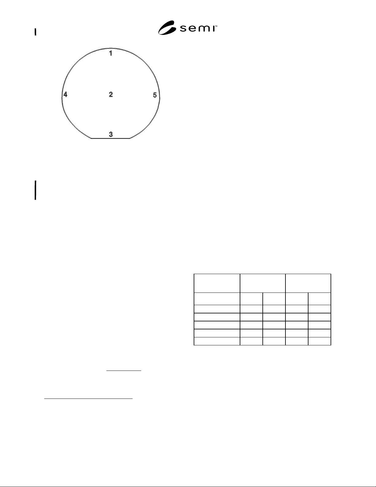
thickness at Point 2, at the wafer center as shown in
Figure 1, is the nominal film thickness for the wafer.
Recommended: SEMI MF95, suitably modified for use
with SOS structures.
7.2.2 Layer Thickness Variation — Unless otherwise
specified, the radial thickness variation shall be
determined from values measured at the center and
edge locations, as shown in Figure 1. Points 1, 3, 4, and
5 are located 6 mm in from the wafer periphery and
define the location of the edge measurements. All
thickness values must be within the specified range. For
example, for a film specified at 0.50 µm ± 10%, all
readings at points 1–5 must be within the range from
0.45 to 0.55 µm.
SEMI M4-1103 © SEMI 1978, 2003 3
Figure 1
Measurement Points for Determination of Layer
Thickness Variation
7.2.3 Resistivity — Determine by a method agreed
upon between supplier and purchaser. Contacting
method: SEMI MF374; Non-contacting method: SEMI
MF673.
7.2.4 Radial Resistivity Variation — Determine in
accordance with sampling plan A of SEMI MF81.
7.2.5 Film Crystallinity — Determine by the following
or an alternative method as agreed between supplier and
purchaser.
7.2.5.1 SOS films can display varying degrees of haze
due to polycrystalline silicon deposits in the film.
These polycrystalline deposits can result from improper
deposition temperatures, substrate surface
contaminants, or contaminants in the reactor or reactor
gases.
7.2.5.2 Haze can be seen visually and can be
quantitatively measured by ultraviolet light reflectance
spectroscopy or by x-ray diffraction (pole figure)
measurements.
3
The ultraviolet light reflectance (UVR)
value is commonly measured to determine the film
crystalline quality. In this technique, measure the
relative reflectance at two wavelengths, 280 and 440
nm, using a clean, polished (100) silicon substrate as
the reference as in the following example:
ref
SOSref
R
RR
R
||
280
−
=∆
3 Currently, there is no standardized method for this procedure. The
procedure is described in: M.T. Duffy, et al, Semiconductor
Measurement Technology: Method to Determine the Quality of
Sapphire, National Institute of Standards and Technology Report No.
NBS SP400-62,August 1980. Available from the National Technical
Information Service, Springfield, VA, as PB80-212830. See also:
M.T. Duffy, et al, J. Crystal Growth 58 (1982) 10.
7.2.5.3 Record the difference between the two
reflectance values, R
280
–R
440
, as the UVR value. For
films in the thickness range 0.5 to 0.8 µm, the R
280
–R
440
value shall be less than 15 units. This value is an
average of 5 points measured in the wafer as shown in
Figure 1. The edge measurements are located at 12.5
mm in from the wafer periphery.
7.2.5.4 For thinner films from 0.2 to 0.6 µm, the
reflectance value at the single wavelength of 280 nm
can be used.
7.2.5.5 X-ray pole figure analysis measures the volume
concentration of microtwins, as % (111), in the silicon
film.
7.2.5.6 The ultraviolet reflectance values and pole
figure values are dependent on film thickness, so
specified limits are listed for each film thickness in
Table 1.
7.2.6 Microparticulate Density — SOS films can
display varying degrees of surface cleanliness as
viewed with a microscope. Small particles trapped in
the film can cause yield losses in some devices. Deter-
mine the density of small particles by counting the
particles observed during an X-Y scan across the wafer
using Normarski interference contrast microscopy at
100×. For particles greater than 2 µm in diameter, the
particle density shall be less than 2 defects per square
centimeter, excluding the outer 6 mm of the wafer
periphery.
Table 1 Ultraviolet Reflection and X-Ray Pole Figure
Values
Film Thickness
Average Value,
(MAX)
1 Peripheral Value,
(MAX)
µm ∆R
280
%(111) ∆R
280
%(111)
0.20 15 7.0 23 11.5
0.30 17 5.5 28 9.5
0.40 21 5.0 33 8.0
0.50 27 4.5 42 7.0
0.60 32 4.0 51 6.5
SEMI M4-1103 © SEMI 1978, 2003 4
7.2.7 Surface Defects and Contamination — Determine
by methods agreed upon between user and supplier.
SEMI MF154 is a useful guide for defining a variety of
surface features and establishing commonly understood
terms for describing surface defects and contamination.
SEMI MF523 is also recommended (see Note 5).
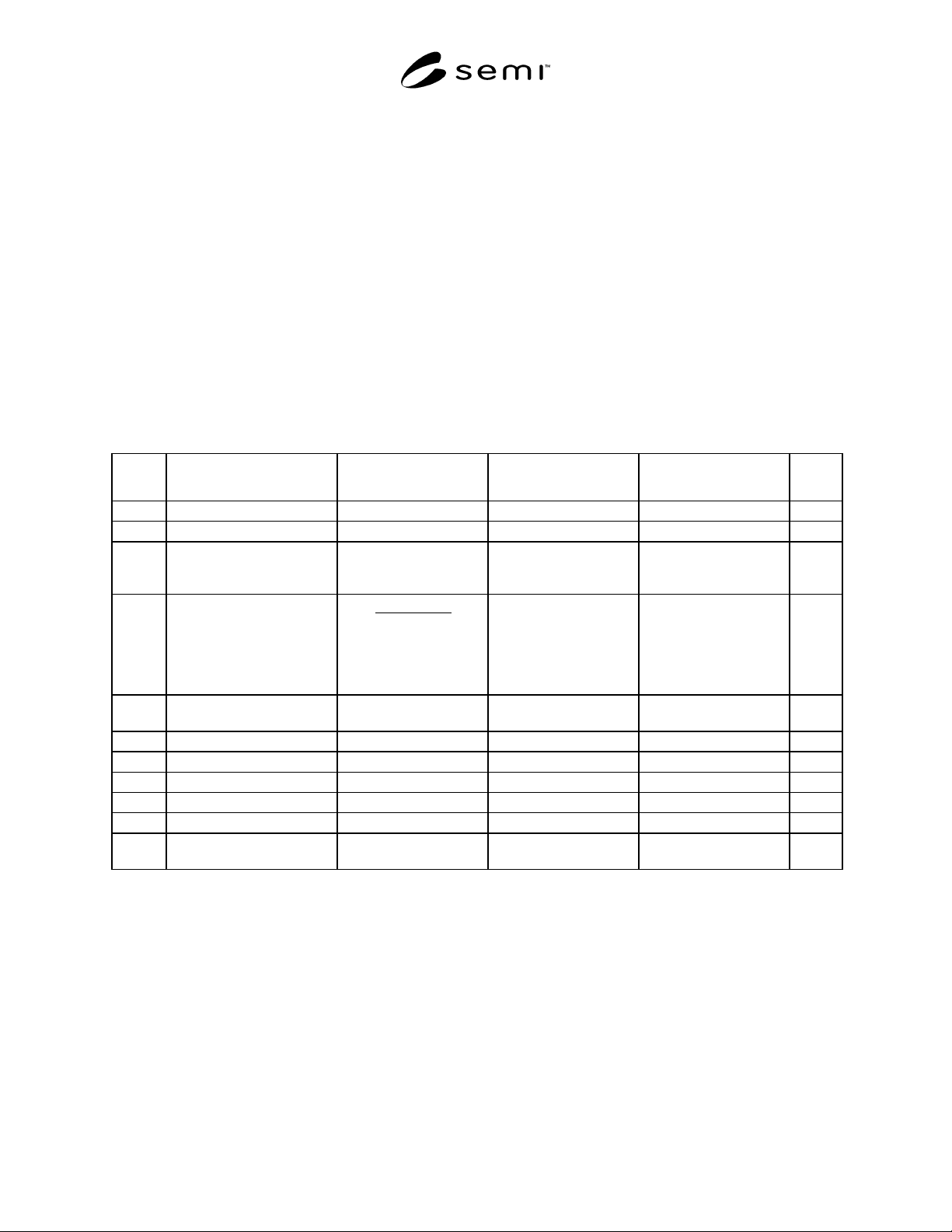
Recommended maximum levels of surface defects and
contamination are listed in Table 2.
NOTE 4: SOS wafers are susceptible to surface damage. The
thin film on the hard sapphire substrate may be damaged
physically in ways that are not immediately evident. Special
care must therefore be used in the selection and execution of
measurement procedures.
NOTE 5: In SEMI MF523, defects commonly found in
silicon wafers are defined. Some of these terms do not apply
to SOS wafers, but are included in Table 2 to provide a
convenient reference point to the silicon wafer and epitaxial
wafer standards. In this case, the recommended maximum
acceptable limit is shown as N.A. (not applicable).
8 Sampling
8.1 Unless otherwise specified, ASTM Practice E 122
shall be used. When so specified, appropriate sample
sizes shall be selected from each lot according to
ANSI/ASQC Z1.4-1993. Each quality characteristic
shall be assigned an acceptable quality level (AQL) and
lot total percent defective (LTPD) value in accordance
with ANSI/ASQC Z1.4-1993 definitions for critical,
major, and minor classifications. If desired and so
specified in the contract or order, each of these
classifications may alternatively be assigned cumulative
AQL and LTPD values. Inspection levels shall be
agreed upon between user and supplier.
Table 2 Recommended Maximum Surface Defects Levels by Non-Destructive Means
ITEM
CHARACTERISTICS
MAX ACCEPTABLE
LIMIT
TEST METHOD
DEFECT DEFINITION
PER
NOTES
1 STACKING FAULTS N.A. 2
2 SLIP N.A. 2
3 PROTRUDING DEFECTS
(Including spikes, hillocks,
pyramids, and inclusions)
N.A. 2
4 PITS Diameter No.
2" 4
3" 9
100 mm 15
125 mm 20
150 mm 25
SEMI MF523 SEMI MF154 1, 3
5 SCRATCHES Cumulative L
1/2 wafer radius
SEMI MF523 SEMI MF154 1, 3
6 CRACKS, FRACTURES None SEMI MF523 SEMI MF154 5
7 ORANGE PEEL N.A. 2
8 EDGE CHIPS Max No. 2 SEMI MF523 SEMI MF154 2
9 EDGE CROWN N.A. 2
10 HAZE None SEMI MF523 SEMI MF154 1, 6
11 FOREIGN MATTER
FINGER PRINTS
None SEMI MF523 SEMI MF154 1, 7
NOTE 1: The outer 4 mm annulus is excluded from these criteria.
NOTE 2: These defects are not observed in SOS wafers. Terms remain for convenient reference to epitaxial silicon wafer specification.
NOTE 3: Ninety percent of the wafers shall be free of these defects. Balance of wafer may have defects at these limits.
NOTE 4: All chips shall be beveled. Maximum penetration 3 mm. Pointed apex chips none. Chips less than 0.4 mm (0.015 in.) shall not be
counted. See SEMI M3, Table R1-1.
NOTE 5: Cracks are observed in sapphire as fractures or as surface separations along cleavage planes.
NOTE 6: Haze refers to the presence of polycrystalline silicon deposits in the film, as described in Section 7.2.5. Haze shall not be visible under
lighting conditions of ASTM F 523.
NOTE 7: Particulate matter easily removed by industry-accepted cleaning techniques shall not constitute foreign matter.