semi合集-English.pdf - 第6006页
SEMI P43-0304 © SEMI 2004 15 allowing compensation of area gain and area los s. In case of, e.g., corner area devation uniformity , line-edge roughness will influence th e measurement result. NOTICE: SEMI makes no warran…
SEMI P43-0304 © SEMI 2004 14
8.4.2.1 In the center-of-gravity (COG) method the
COG of actual and nominal features are superimposed.
8.4.2.2 In the area based method the absolute feature
area deviation between the actual and nominal features
is minimized.
8.4.2.3 In the line-edge based method, alignment is
performed by minimizing the distance between multiple
actual and nominal edges.
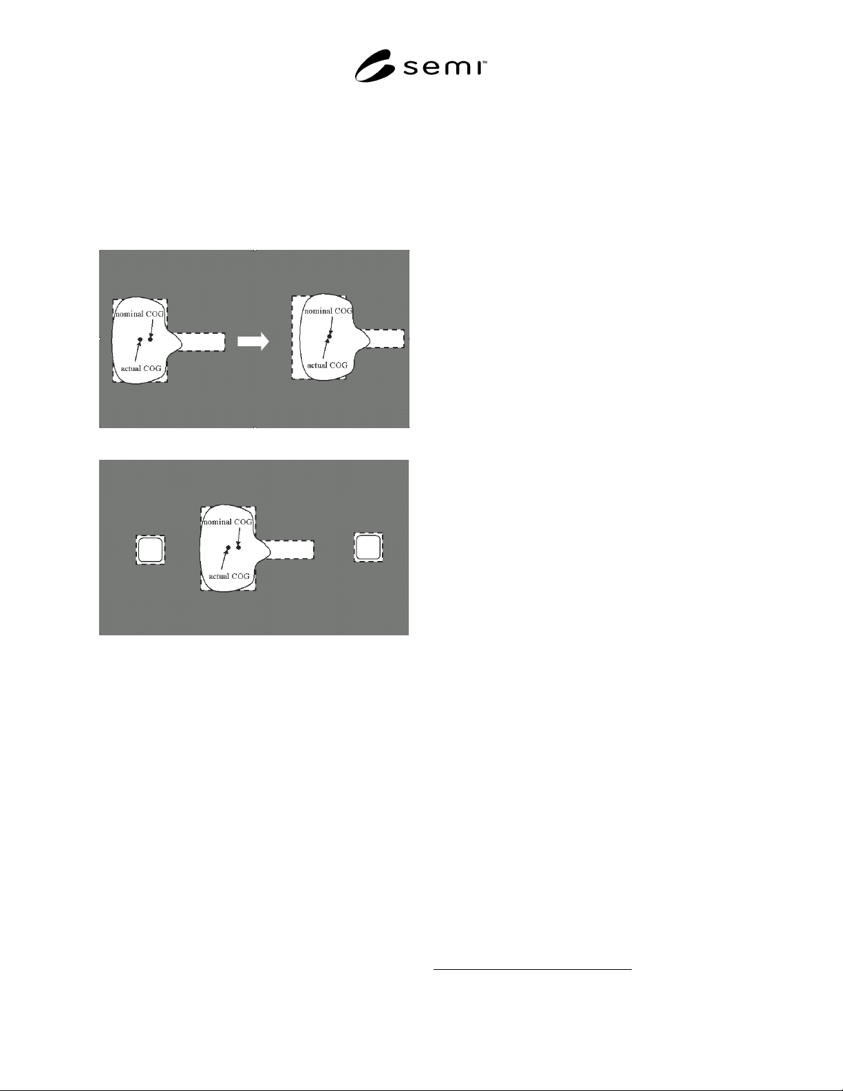
(a)
(b)
Figure 22
Alignment of nominal and actual feature
(a) by center of gravity (COG) only, left is the
intended overlay, right is actual overlay from the
COG method, leading to an incorrect result.
(b) by the use of alignment markers.
8.4.3 Alignment is preferably done on dedicated
alignment features (markers), which are symmetric and
not clipped, and their position does not suffer from the
resolution of the imaging process. Crosses are typically
used, as they have X and Y components, which can be
used to correct for rotational error if only one marker
were present.
8.4.4 Additional markers allow for more accurate
rotational compensation and decouple magnification
errors of the feature to be measured from sizing errors.
8.4.5 If no markers are present, one of the methods
above can be attempted on the feature to be measured
or on other features in the ROI, but in such situation
alignment may be less accurate, especially if these
features are clipped (see Figure 22).
8.5
Measured Values
8.5.1 By analogy to Section 7 (1D Mask Qualification
Terminology) a measured qualification parameter can
be defined for every 2D (true) qualification parameter
defined in Section 8.2. In Section 7 this was done
immediately after the definition of the true parameter,
whereas here the measured parameter is treated in a
generic way. Thereby, one 2D qualification parameter
is used for the explanation, i.e., measured corner area
difference and its uniformity, as examples for all other
2D qualification parameters and their uniformity.
NOTE 43: The most critical feature in terms of impact of the
measurement details to the measured values is the size of a
contact near the resolution limit of the metrology tool and of
the mask patterning process.
8.5.2 measured corner area difference — measured
value of corner area difference, stating as mandatory
information, in addition to that of corner rounding
(Section 8.2.3.1):
• calibration method used
4
,
• measurement method used (SEM, optical
reflection, optical transmission, AFM, etc.) and its
resolution limit,
• edge detection algorithm and parameters,
• precision (SEMI P24),
and as optional information :
• measurement tool (vendor, model or any tool
specific options).
8.5.3
measured corner area difference uniformity —
measured value of corner area difference uniformity,
thereby stating as mandatory information in addition to
that of corner area difference uniformity and of
measured corner area difference:
• the number of measurement points used,
and as optional information:
• the spatial distribution of measurement locations,
e.g., by coordinates of measurement locations.
DEFAULT is spread evenly over the measurement
area.
NOTE 44: Edge roughness, either originating from the
process (Note 19 in Section 8.2.2) or from the measurement
technique used, may influence the measurement result. This
is not the case for the two examples treated above, as the
difference parameter filters out the effect of roughness by
4 See reference document in Section 4.2.

SEMI P43-0304 © SEMI 2004 15
allowing compensation of area gain and area loss. In case of,
e.g., corner area devation uniformity, line-edge roughness
will influence the measurement result.
NOTICE: SEMI makes no warranties or
representations as to the suitability of the standards set
forth herein for any particular application. The
determination of the suitability of the standard is solely
the responsibility of the user. Users are cautioned to
refer to manufacturer’s instructions, product labels,
product data sheets, and other relevant literature,
respecting any materials or equipment mentioned
herein. These standards are subject to change without
notice.
By publications of this standard, Semiconductor
Equipment and Materials International (SEMI) takes no
position respecting the validity of any patent rights or
copyrights asserted in connection with any items
mentioned in this standard. Users of this standard are
expressly advised that determination of any such patent
rights or copyrights, and the risk of infringement of
such rights are entirely their own responsibility.
Copyright by SEMI® (Semiconductor Equipment and Materials
International), 3081 Zanker Road, San Jose, CA 95134. Reproduction o
f
the contents in whole or in part is forbidden without express written
consent of SEMI.

SEMI INTERNATIONAL STANDARDS
PACKAGING
Semiconductor Equipment and Materials International