semi合集-English.pdf - 第5021页
SEMI M18-0704 © SEMI 1990, 2004 7 7 Testing Level and Certification 7.1 Material order ed using this format shall be tested and/or certified to the limits set forth in the individual criteria. 7.2 Th e actual testing lev…
SEMI M18-0704 © SEMI 1990, 2004 6
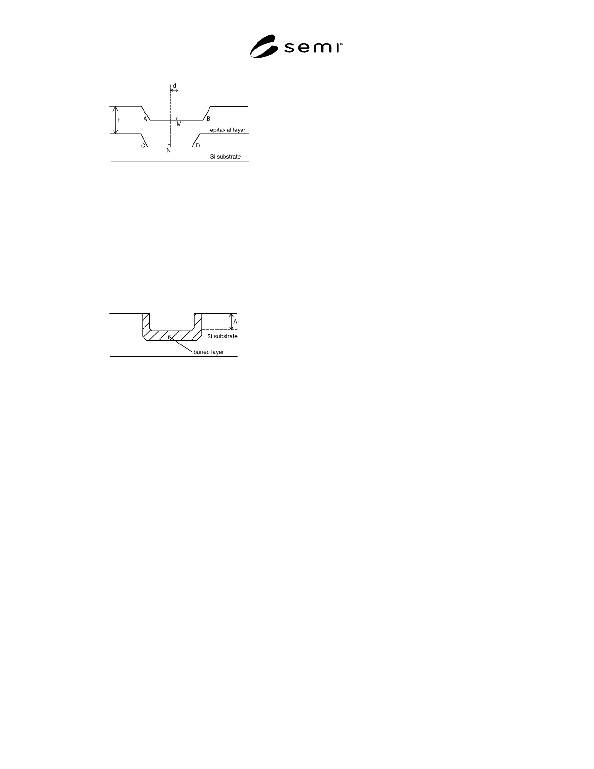
Figure 5
Cross-Section View of Epitaxial Wafer Showing the
Pattern Shift, d. Not to scale: AM = MB and CN =
ND
4.3.5 pattern step height — difference in vertical
position of the diffused (buried layer) surface and the
original substrate surface, after removal of oxide.
NOTE 5: Pattern step height, A, is specified as a nominal
value, X, and a tolerance ± Y, both in nm. See Figure 5.
Figure 6
Cross-Sectional View of Epitaxial Substrate After
Oxide Removal but Before Deposition of the
Epitaxial Layer Showing the Pattern Step Height, A
4.4 Terms Related to Annealed Wafers
4.4.1 annealed wafer — wafer that has defects (COP)
free zone near the surface produces by high temperature
annealing.
4.4.1.1 hydrogen annealed wafer — annealed wafer
produced under hydrogen atmosphere.
4.4.1.2 argon annealed wafer — annealed wafer
produced under argon atmosphere.
4.5 Terms Related to SOI Wafers
4.5.1 SOI wafer — wafer that has a buried oxide layer
(BOX).
4.5.1.1 SIMOX wafer — SOI wafer made by oxygen
implantation and high temperature annealing
technology.
4.5.1.2 Bonded wafer — SOI wafer made by bonding
two silicon wafers with an insulating layer between
them. The insulating layer is typically grown oxide.
5 Use of the Form
5.1 Different parts of the specification form are used
for ordering different types of silicon wafers:
5.1.1 For polished wafers, complete Parts 1 and 2.
5.1.2 For epitaxial wafers, complete Parts 1, 2, and 3.
5.1.3 For epitaxial wafers with buried layer, complete
Parts 1, 2, 3, and 4.
5.1.4 For annealed wafers, complete parts 1, 2, and 5.
5.1.5 For SOI wafers, complete Parts 1, 2, and 6. If
necessary, complete Parts 3, 4, or 5.
5.2 In all cases, items listed as required must have a
value or choice indicated to minimally specify the
material.
5.3 Certain required dimensional items may be
specified as a group according to the standard values
presented in the applicable SEMI specification, or they
may be specified individually.
5.4 Visual inspection criteria may be specified as a
group according to the standard values listed in the
applicable SEMI specification, or they may be specified
individually.
5.5 For either dimensional values or visual inspection
criteria, the appropriate SEMI specification may be
marked and an optional line item (or items) marked as
well. In this case, the value marked on each individual
line item takes precedence over the standard value.
5.6 If the suggested form included in this format is not
reproduced and used as a fill-out form, the items and
responses must be adequately identified so that the
information and requirements are clear to all parties.
6 Test Methods
6.1 Measurements shall be made or certifiable to the
ASTM, JEITA, JIS, or DIN standard test method as
cited in Table 1.
6.2 When standard test methods from different
geographic regions are available, the default method
shall be the method in common usage for the region of
the purchaser of the wafer.
6.3 If several different standard test methods for an
item are commonly used within a region, a specific
entry must be made to identify which method of test is
applicable.
6.4 If no standard test method for an item is available,
the test procedure must be specified.
SEMI M18-0704 © SEMI 1990, 2004 7
7 Testing Level and Certification
7.1 Material ordered using this format shall be tested
and/or certified to the limits set forth in the individual
criteria.
7.2 The actual testing level, whether the test is
performed on all wafers, a sample of the wafers, special
test pieces representing all portions of the material, or a
sample of the test pieces, may be specified using this
format.
7.3 In some cases, the material may be certified as
“capable of meeting” certain requirements. In this
context, the supplier is not required to perform the tests
outlined in this format. However, if the purchaser
performs the test and the material fails to meet the
requirement, the material may be subject to rejection.
8 EDI Codes and Sub-Parameter Codes
8.1 The EDI Codes for each parameter are listed in the
following Table. Where necessary for clarity,
additional sub-parameters are listed. These sub-
parameter identify a specific measurement technique or
method to be used.
8.2 If additional codes are required in the future, they
will be added to the table, beginning with the next
available EDI code identifier. This will allow the table
to be rearranged for clarity while maintaining unique
and consistent EDI codes for existing parameters.
Table 2 provides a numerically sorted list of the EDI
Codes.
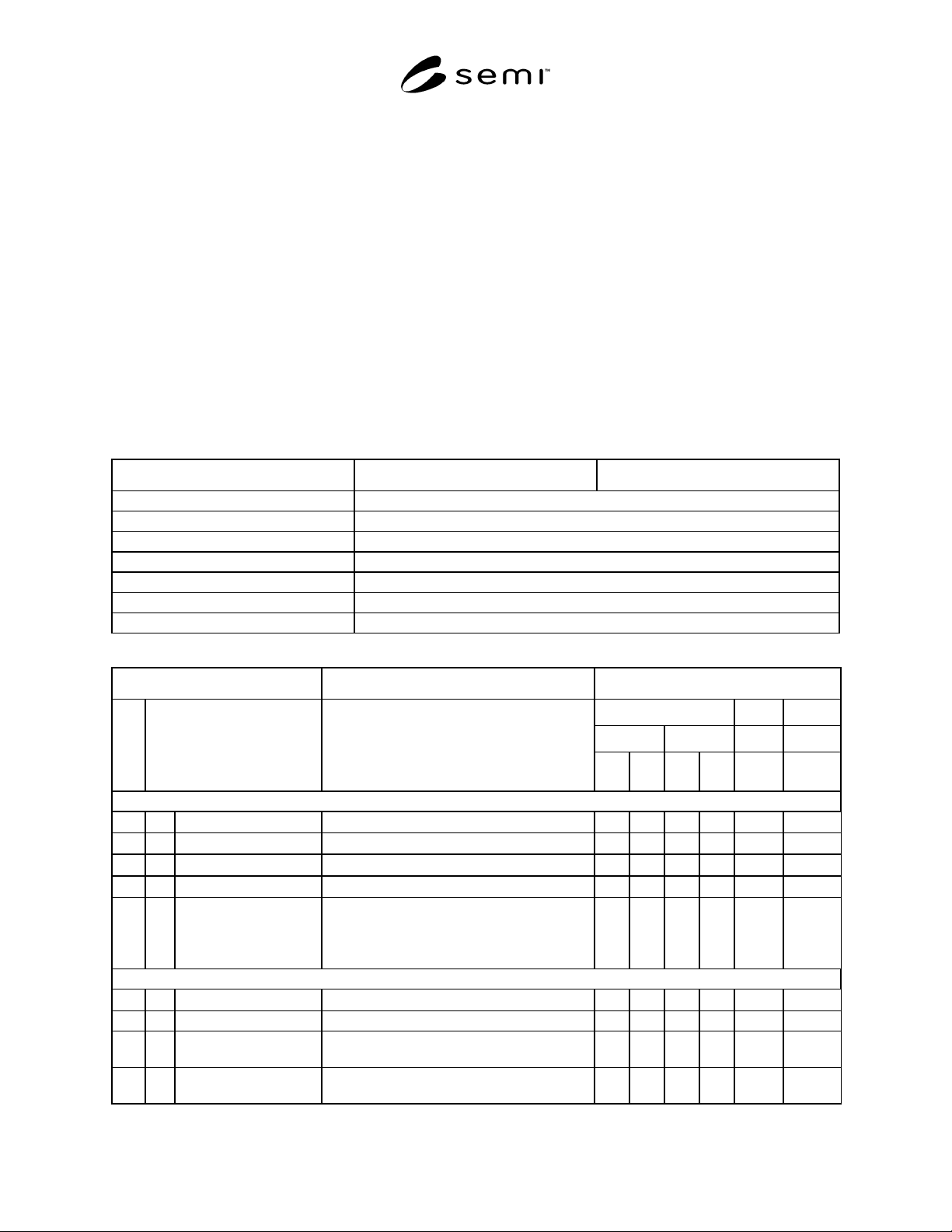
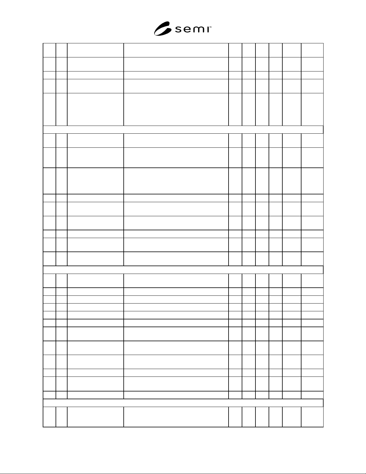
SEMI Silicon Wafer Specification Form For Order Entry (Page 1)
Part 1 General Information
I
TEM
S
I
NFORMATIO
N
D
ate:
Customer Name
Purchase Order Number
Line Number
Item Number
General Specification Number
Revision Level
Part Number/Revision
Part 2 Polished Wafer
CUSTOMER:
P
ART NUMBER: REVISION
D
ATE:
TESTING LEVEL EDI Sub
WAFER TEST PIECE
Code Param
REQUIRED
ITEM SPECIFICATION
100% SAMP
LE
100% SAMP
LE
ID ID
1. GENERAL CHARACTERISTICS
♦
1.1 Growth Method [ ]Cz [ ]FZ [ ]MCz 100001
♦
1.2 Crystal Orientation [ ](100) [ ] (111) [ ] ( ) 100002
♦
1.3 Conductivity Type [ ]p [ ]n 100003
♦
1.4 Dopant [ ]B [ ]Phos [ ]Sb [ ]As [ ]NTD 100004
1.5 Nominal Edge Exclusion
Distance for Fixed
Quality Area
Applies to Sections 6.10–6.14; 11 [ ]3 mm;
[ ]5 mm; [ ]Other__mm
Applies to Sections 7, 8, 12, 13 [ ]3 mm; [ ]5
mm; [ ]Other__mm (except edge defects)
100005
2. ELECTRICAL CHARACTERISTICS
♦
2.1 Resistivity
Nominal [ ] ± Tolerance [ ] Ω−cm
100006
Measurement Position [ ]Center Point; [ ]Other:
Measurement Method [ ]SEMI MF81; [ ]SEMI MF673; [ ]JIS H 612;
[ ]JEIDA 18; [ ]DIN 50431
2.2 Radial Resistivity
Variation (RRG)
Not greater than [ ]% 100007
SEMI M18-0704 © SEMI 1990, 2004 8
Measurement Position SEMI MF81 Fig. 1 - [ ]A, [ ]B, [ ]C, [ ]D;
[ ] JEIDA 18; [ ]DIN 50435
Calculation Method [ ]SEMI MF81; [ ]JEIDA 18; [ ]DIN 50435;
[ ]Other:
2.3 Resistivity Striations Not greater than [ ]% 100008
2.4 Minority Carrier
Lifetime
Greater than [ ]µs
100009
Test Method SEMI MF28 [ ]A, [ ]B; SEMI MF391 [ ]A,
[ ]B;
[ ]SEMI MF1388; [ ]SEMI MF1535; [ ]JEIDA
53;
[ ]JIS H604; [ ]DIN 50440; [ ]Other
3. CHEMICAL CHARACTERISTICS
3.1 Oxygen Concentration Nominal [ ] ± Tolerance [ ]; [ ] × 10
17
cm
-3
;
[ ]ppma
100010
Calibration Factor [ ]SEMI MF1188; [ ]ASTM F121(79);
[ ]ASTM F121(83); [ ] JEIDA 61;
[ ]DIN 50438/1; [ ]Other ____
Measurement Method IR (Interstitial): [ ] SEMI MF1188; [ ] SEMI
MF1619; [ ] JEIDA 61; [ ] DIN 50438-1
SIMS (Total): [ ]SEMI MF1366
[ ]GFA (Total)
3.2 Radial Oxygen Variation Not greater than [ ]% 100011
Measurement Position SEMI MF951 Plan [ ]A, [ ]B, [ ]B1, [ ]C, [ ]D;
[ ]Other:__
Calculation Method SEMI F951 Plan [ ]A, [ ]B, [ ]B1, [ ]C, [ ]D;
[ ] Other:__
3.3 Carbon Concentration Not greater than [ ] [ ]ppma; [ ] × 10
16
cm
-3
100012
Measurement Method [ ]SEMI MF1391; JEIDA 56; [ ]DIN 50438/2;
[ ]Other:____
3.4 Boron Concentration in
Heavily Doped n-type Si
Not greater than [ ] ppba 100013
4. STRUCTURAL CHARACTERISTICS
4.1 Dislocation Etch Pit
Density
[ ]Not greater than [ ]/cm
2
100014
4.2 Slip [ ]None [ ]Other ___ 100015
4.3 Lineage [ ]None [ ]Other ___ 100016
4.4 Twin [ ]None [ ]Other ___ 100017
4.5 Swirl [ ]Not greater than [ ]% of wafer area 100018
4.6 Shallow Pits Not greater than [ ]/cm
2
100019
4.7 Oxidation Induced
Stacking Faults (OSF)
Not greater than [ ]/cm
2
100020
Test Cycle ASTM F 416 Cycle-[ ]1 [ ]2 [ ]3;
[ ] SEMI MF 1727; [ ]Other:__
4.8 Oxide Precipitates
(BMD)
Range: [ ] to [ ]
Unit: [ ] cm
2
[ ] cm
3
100021
Test Cycle SEMI MF1239 [ ]A, [ ]B; [ ] Other:_____
4.9 Interstitial Oxygen
Reduction (∆O
I
)
Range: [ ] to [ ] [ ]ppma, [ ] × 10
17
cm
-3
100162
Test Cycle SEMI MF1239 [ ]A, [ ]B; [ ] Other:_____
5. WAFER PREPARATION CHARACTERISTICS
5.1 Wafer ID Marking [ ]None; [ ]SEMI M12; [ ]SEMI M13;
[ ]SEMI T1; [ ]SEMI T2; [ ] SEMI T7;
[ ]Other:_____
100022