semi合集-English.pdf - 第5092页
SEMI M23.6-0703 © SEMI 2003 1 SEMI M23.6-0703 SPECIFICATION FOR ROUND 150 mm POLISHED MONOCRYSTALLINE INDIUM PH OSPHIDE WAFERS (NOTCHED) This specification was technically approved by the Global Com pound Semiconductor M…
SEMI M23.5-1000 © SEMI 20001
SEMI M23.5-1000
SPECIFICATION FOR ROUND 100 mm POLISHED
MONOCRYSTALLINE INDIUM PHOSPHIDE WAFERS FOR
ELECTRONIC AND OPTOELECTRONIC DEVICE APPLICATIONS (V-
GROOVE OPTION)
This specification was technically approved by the Global Compound Semiconductor Committee and is the
direct responsibility of the North American Compound Semiconductor Committee. Current edition approved
by the North American Regional Standards Committee on August 28, 2000. Initially available at
www.semi.org September 2000; to be published October 2000.
NOTE: The complete specification for this product includes all requirements of SEMI M23.
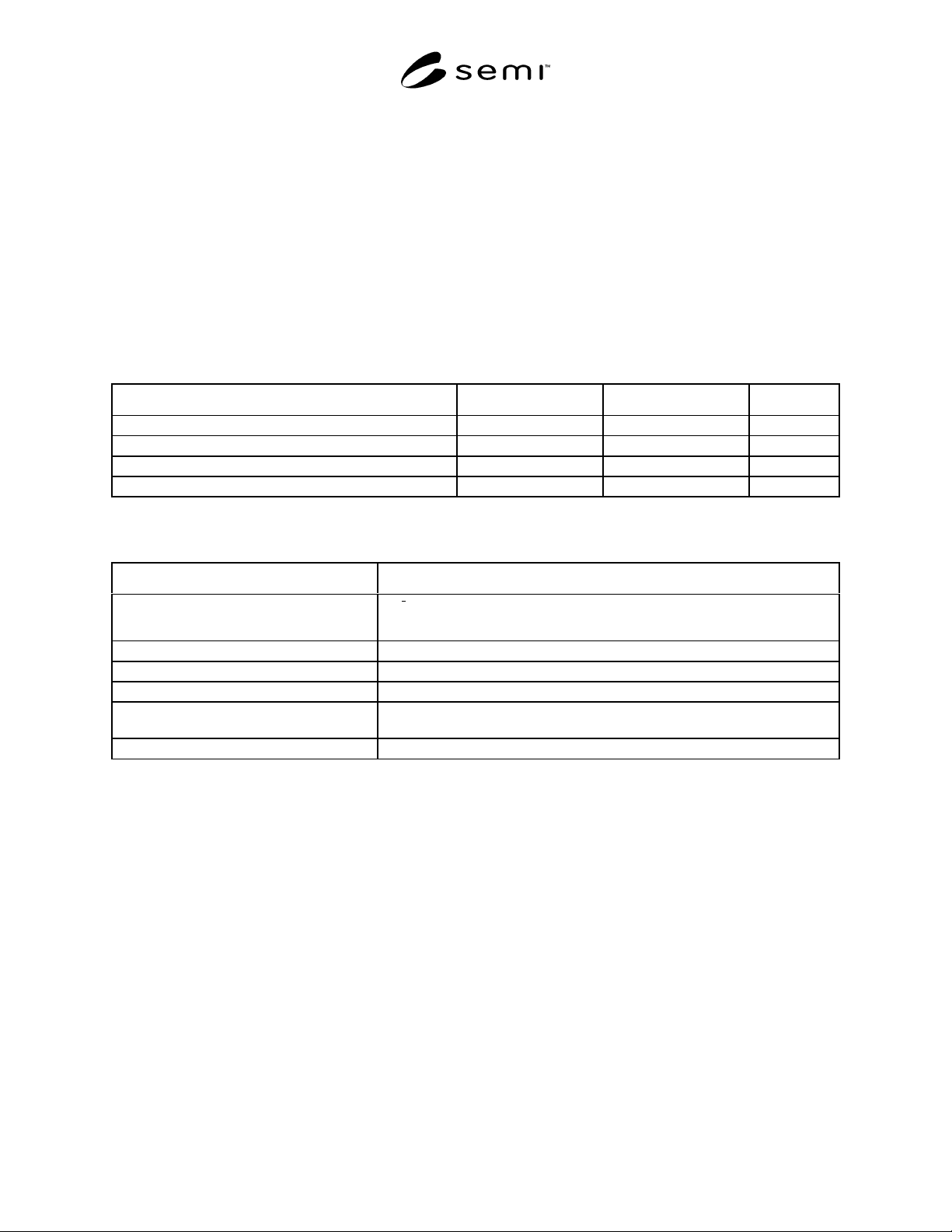
Table 1 Dimension and Tolerance Requirements
Property Dimension Tolerance Units
DIAMETER (See NOTE 1.) 100.0 ± 0.5 mm
THICKNESS, CENTER POINT 625 ± 25 µm
PRIMARY FLAT LENGTH 32.5 ± 2 mm
SECONDARY FLAT LENGTH 18 ± 2 mm
NOTE 1: The diameter standard means that the dimension is centered to this value.
Table 2 Orientation and Flat Location Requirements
Property Requirement
PRIMARY FLAT ORIENTATION
)101( ± 0.5° (see NOTE 1) under a Phosphorus facet. The primary flat shall be
perpendicular to the “V” etch figure. (See NOTE 2.)
SECONDARY FLAT ORIENTATION (011), 90°± 5° counterclockwise from the primary flat.
SURFACE ORIENTATION (See NOTE 3.)
A. { 100} (see
NOTE 1) ± 0.5° (See Figure 2 in SEMI M23.)
B. { 100} (see NOTE 1) off 2° ± 0.5° toward the (110) plane which is between the
primary and secondary flats (See Figure 4 in SEMI M23.)
ORTHOGONAL MISORIENTATION ± 5° (See Figure 5 in SEMI M23.)
NOTE 1: See Table 1 in SEMI M23.
NOTE 2: See Figure 2 in SEMI M23, which shows the orientation of the V-groove figure relative to crystallographically anisotropic pits (see
NOTE 4).
NOTE 3: The frame of reference is the (100) plane of the crystal. It is the wafer normal that is tilted toward the (110) plane of the crystal.
NOTE 4: Relating to the etchant used for identifying V-groove and/or dovetail direction, see reference: “HBr-K
2
Cr
2
O
7
- H
2
O etching system for
indium phosphide” J.L.Weyher, et al. Materials Science and Engineering B28 (1994) 488–492.
NOTICE: These standards do not purport to address safety issues, if any, associated with their use. It is the
responsibility of the user of these standards to establish appropriate safety and health practices and determine the
applicability of regulatory limitations prior to use. SEMI makes no warranties or representations as to the suitability
of the standards set forth herein for any particular application. The determination of the suitability of the standard is
solely the responsibility of the user. Users are cautioned to refer to manufacturer’s instructions, product labels,
product data sheets, and other relevant literature respecting any materials mentioned herein. These standards are
subject to change without notice.
The user’s attention is called to the possibility that compliance with this standard may require use of copyrighted
material or of an invention covered by patent rights. By publication of this standard, SEMI takes no position
respecting the validity of any patent rights or copyrights asserted in connection with any item mentioned in this
standard. Users of this standard are expressly advised that determination of any such patent rights or copyrights, and
the risk of infringement of such rights, are entirely their own responsibility.
Copyright by SEMI® (Semiconductor Equipment and Materials
International), 3081 Zanker Road, San Jose, CA 95134. Reproduction o
f
the contents in whole or in part is forbidden without express written
consent of SEMI.
SEMI M23.6-0703 © SEMI 2003 1
SEMI M23.6-0703
SPECIFICATION FOR ROUND 150 mm POLISHED
MONOCRYSTALLINE INDIUM PHOSPHIDE WAFERS (NOTCHED)
This specification was technically approved by the Global Compound Semiconductor Materials Committee
and is the direct responsibility of the Japanese Compound Semiconductor Materials Committee. Current
edition approved by the Japanese Regional Standards Committee on April 28, 2003. Initially available at
www.semi.org June 2003; to be published July 2003.
1 Purpose
1.1 This specification defines properties of 150 mm
monocrystalline InP substrates, in agreement with
presently established industry practice. It uniquely
defines those mechanical parameters that do not need,
for technical reasons, a choice of different values.
2 Scope
2.1 The parameters defined include the values and
tolerances of wafer diameter, thickness and surface
orientation. The position and depth of the notch and
laser marking are also specified.
2.2 The complete specification of this product includes
the requirements of SEMI M23, excluding those that
are not relevant to this specification (e.g., flat
positions).
NOTICE: This standard does not purport to address
safety issues, if any, associated with its use. It is the
responsibility of the users of this standard to establish
appropriate safety and health practices and determine
the applicability of regulatory or other limitations prior
to use.
3 Referenced Standards
3.1 SEMI Standards
SEMI M12 — Specification for Serial Alphanumeric
Marking of the Front Surface of Wafers
NOTICE: Unless otherwise indicated, all documents
cited shall be the latest published versions.
4 Terminology
None.
5 Physical Requirements
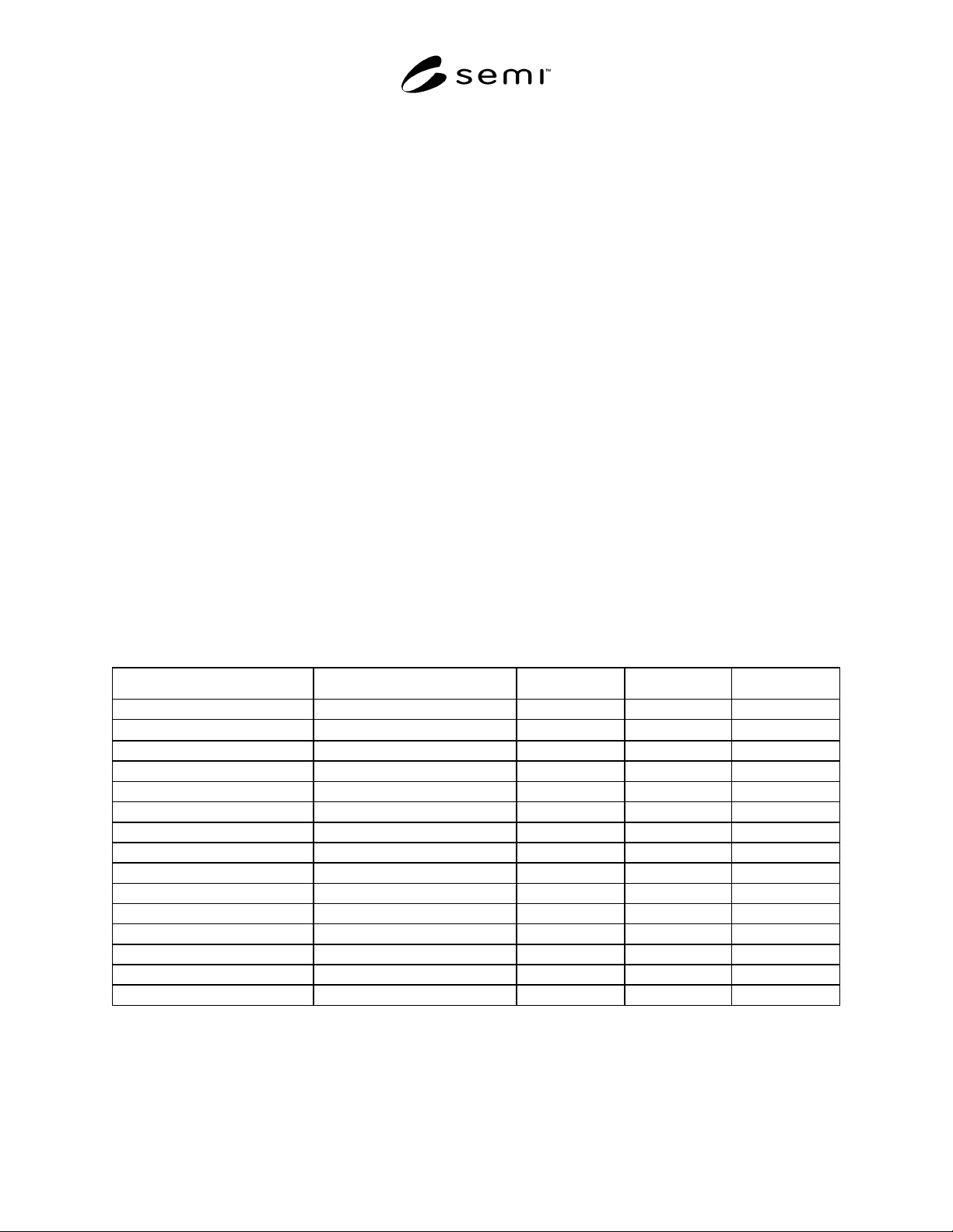
Table 1 Physical Requirements
Property Specification Tolerance Unit Reference
WAFER
Diameter 150.0
± 0.5
mm
Thickness, center point 675 ± 25 µ m
Surface orientation A (100) 0.5 max. degrees Figure 2
Surface orientation B
Tilt 2 off (100) towards (110) ± 0.5 degrees Figure 3
Orthogonal misorientation 0 ± 5 max. degrees Figure 4
NOTCH
Orientation [010] ± 2 degrees Figure 1
Depth 1.00 + 0.25, -0.00 mm Figure 5
Opening angle 90 + 5, -1 degrees Figure 5
LASER MARKING
Surface front side
Position adjacent to notch Figure 6
Mandatory content check characters SEMI M12
SEMI M23.6-0703 © SEMI 2003 2
_
(111)
P
_
(111)
P
_
(011)
_
(001)
(010)
(110)
(101)
(001)
(011)
_
(110)
_ _
(111)
In
(111)
In
_
(011)
_
(101)
(100)
_ _
(011)
Etch Pit
_
(010)
Cross Section of Etch Figure
on Front Face of Wafer
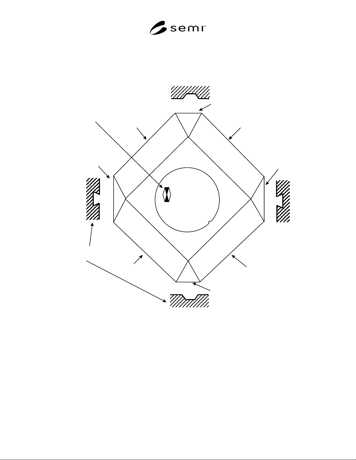
Figure 1
Diagram Shows a InP Wafer with Notch