semi合集-English.pdf - 第7353页
SEMI MF1391-0704 © 2004 5 Figure 1 Carbon-Only Absorbance Spectrum 10.4.1 For double-beam instru ments, position the sample specimen in the sample beam and the reference specimen in the reference beam and collect and plo…

SEMI MF1391-0704 © 2004
4
4
reference slices shall be equal to within ± 0.5 mm (see
Section 10.5).
9.2.4 Surface area large enough such that with respect
to the holders no incident radiation can bypass either
the test or reference specimen.
9.3 The reference specimen must be selected from float
zone silicon with a minimal substitutional carbon
concentration and a carrier concentration such that there
is no measurable free carrier absorption of infrared
radiation in the range from 500 to 2000 cm
−1
.
NOTE 1: A satisfactory method of selecting usable reference
specimens is to prepare polished slices of equal thickness
from many different low-carbon silicon crystals produced by
the float zone method, and then compare them to each other in
an infrared radiation (IR) spectrophotometer. The selection
must be carried out at cryogenic temperatures for cryogenic
measurements. The specimen(s) showing the highest relative
transmittance at 605 cm
−1
at room temperature, or at 607.5
cm
−1
at cryogenic temperatures (below 80 K), can be used as
reference specimen(s).
9.4 Both test and reference specimens must have
resistivity greater than 3 Ω·cm for p-type silicon and
greater than 1 Ω·cm for n-type silicon.
10 Procedure
10.1 Instrumental Checks
10.1.1 With reference to the transmittance spectrum,
establish the 100% transmittance line to measure the
stability and the noise level by one of the following
methods.
10.1.1.1 For double-beam instruments, record the
transmittance spectrum with both the sample and
reference beams empty.
10.1.1.2 For single-beam instruments, record the trans-
mittance spectrum as the ratio of two spectra taken with
the sample beam empty. Take the two spectra at times
separated by at least the time required to load samples
and take two sequential spectra.
10.1.1.3 In both cases, plot the transmittance spectrum
over the wavenumber range covering 500 to 700 cm
−1
to obtain the 100% line.
10.1.1.4 If the 100% transmittance line is 100 ± 0.5%
over the entire range, continue to the next step.
Otherwise, adjust or repair the instrument so as to meet
this criterion.
10.1.2 Establish the 0% transmittance line, (T).
10.1.2.1 For double-beam dispersive (DIR)
instruments, record the transmittance spectrum between
700 and 500 cm
−1
with the sample beam blocked.
10.1.2.2 For FT-IR instruments, collect a background
spectrum with the beam empty. Next, collect a
spectrum with a CaF
2
crystal wafer, 5-mm thick, in the
beam. Obtain the spectrum that is the ratio of the CaF
2
spectrum to the background spectrum, and plot the
percent transmittance spectrum between 700 and 500
cm
−1
.
10.1.2.3 In either of these cases, the 0% transmittance
must not exceed ± 0.5% over the range between 700
and 500 cm
−1
.
10.1.2.4 Alternatively, for FT-IR instruments, plot the
single-beam background spectrum (empty beam only)
from 1000 to 200 cm
−1
. The recorded energy in a
region where the detector is known to give a zero
response (below 300 cm
−1
for most detectors) must not
be greater than 1.0% of the maximum signal in this
region.
4
,
5
10.1.3 To determine the mid-scale linearity of the
instrument obtain a spectrum of the silicon reference
specimen over the wavenumber range from 1600 to
2000 cm
−1
. If the value of the transmittance is not 53.8
± 2% over this wavenumber range, align the sample at a
small angle to the axis of the incoming IR beam, in
order to minimize undesirable reflections between the
silicon surfaces and the spectrometer components.
NOTE 2: This angle may be determined by initially placing
the silicon slice normal to the axis of the incoming beam, and
then gradually tilting the specimen while repeatedly obtaining
the transmittance spectrum above 1600 cm
−1
. The optimum
angle is typically less than 10°.
10.2 Measure and record the thicknesses of the test and
reference specimens to within ± 0.005 mm, at their
centers.
10.3 For room temperature measurements, measure and
record the temperature of the sample chamber to ± 2°C.
At cryogenic temperatures (below 80 K), measure and
record the temperature of the sample holder.
10.4 Obtain the carbon-only absorbance spectrum by
one of the following methods (see Figure 1):
4 Chase, D. B., Applied Spectroscopy 38(4), 491–494 (1984).
5 Hoffman, P., and Knozinger, E., Applied Spectroscopy 41(8),
1303–1306, (1987).
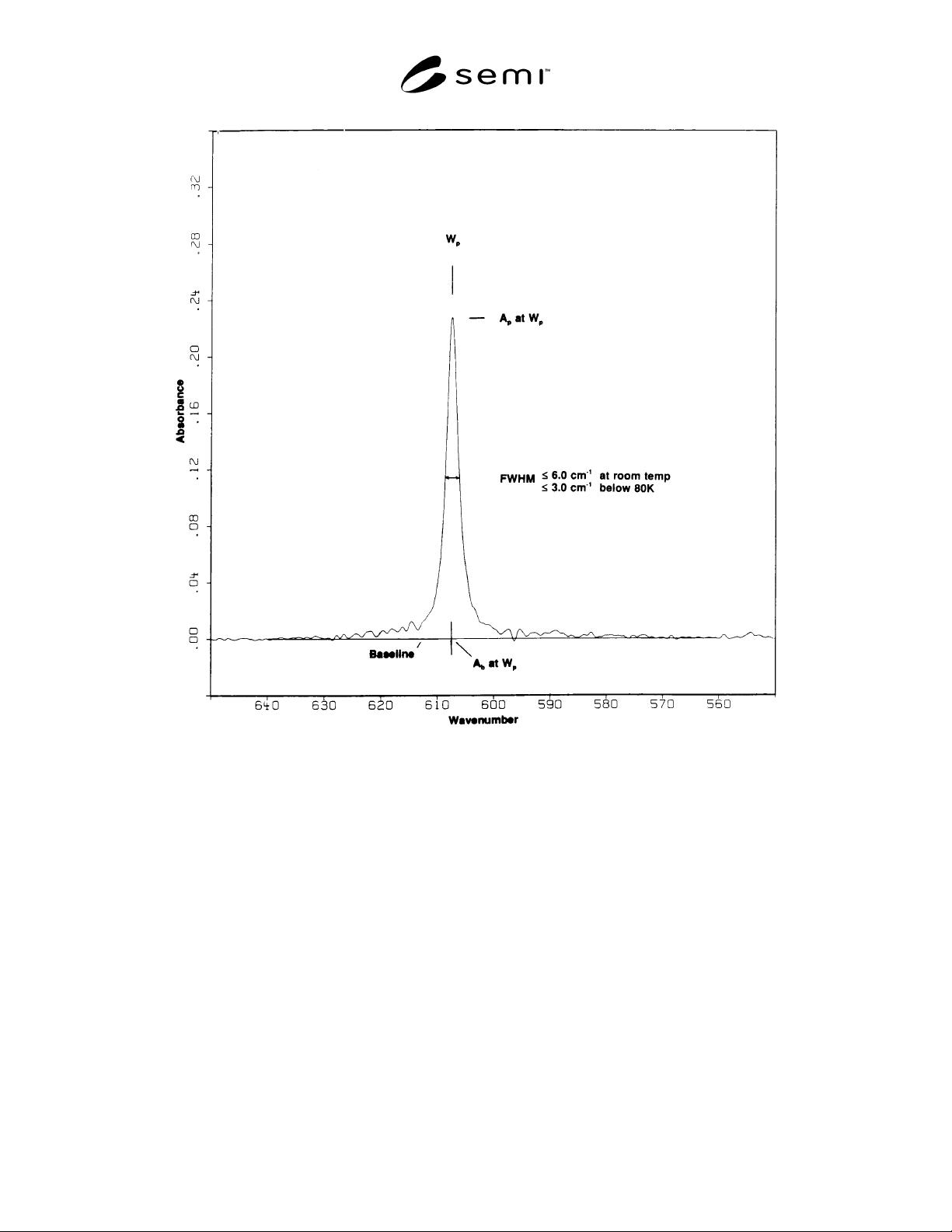
SEMI MF1391-0704 © 2004 5
Figure 1
Carbon-Only Absorbance Spectrum
10.4.1 For double-beam instruments, position the
sample specimen in the sample beam and the reference
specimen in the reference beam and collect and plot the
carbon-only absorbance spectrum over the range of at
least 700 to 500 cm
−1
. Use a resolution of 2 cm
−1
or
better, at 605 cm
−1
, at room temperature, and a
resolution of 1 cm
−1
or better, at 607.5 cm
−1
, at cryo-
genic temperatures (below 80 K). Take spectra with the
sample chamber in a vacuum, dry nitrogen, or dry air.
Position the specimen so that the infrared beam passes
through the center of the specimens.
10.4.2 For single-beam (computer-assisted)
instruments, first collect a background spectrum with
the beam empty, then collect sample and reference
spectra sequentially under the same conditions as given
in Section 10.4.5. Ratio the sample and reference
spectra to the background and convert to absorbance.
Multiply the reference absorbance spectrum by the ratio
of the test specimen thickness to the reference specimen
thickness and subtract this normalized absorbance from
the test specimen absorbance to obtain the carbon-only
spectrum.
NOTE 3: If the user has interactive arithmetic capability,
subtract the reference absorbance spectrum from the sample
absorbance spectrum in a ratio that provides the best flatness
of the non-peak baseline between 560 and 640 cm
−1
. This
eliminates the 2-phonon band due to silicon and gives a
carbon-only spectrum.
10.5 With regard to the plot of the carbon-only
absorbance spectrum over the range from 500 to 700
cm
−1
, define the baseline by drawing a straight line
from 560 to 640 cm
−1
. Use the average in the regions
from 550 to 570 cm
−1
, and 630 to 650 cm
−1
, to define
the endpoints of the straight line.

SEMI MF1391-0704 © 2004
6
6
10.6 For measurements at room temperature, locate the
wavenumber corresponding to the maximum
absorbance in the region from 603 to 607 cm
−1
. For
measurements at cryogenic temperatures (below 80 K),
locate the wavenumber corresponding to the maximum
absorbance in the region from 605 to 609 cm
−1
.
10.6.1 Record the value of that wavenumber, to four
significant figures, as W
p
. Record the maximum
absorbance as A
p
, the absorbance of the absorption
peak.
10.6.2 Record the baseline absorbances, A
b
, as the
value of the baseline defined in 10.5 at W
p
.
10.6.3 Record both A
p
and A
b
to three significant
figures.
10.7 Determine and record the full width at half
maximum (FWHM) of the peak. If the FWHM of the
peak is greater than 6 cm
−1
(room temperature) or 3
cm
−1
(cryogenic temperatures), the spectrum was not
properly obtained, and the instrument needs further
adjustment, or the specimen is under stress. See
Section 3.4 for a list of factors that influence FWHM.
Adjust the instrument in order to achieve the proper
FWHM and repeat the procedure.
10.8 Record the apodization function and the number of
zero-fills used (FT-IR instruments) or the spectral slit
width for dispersive infrared (DIR) instruments.
11 Calculation
11.1 Calculate the absorption coefficient, α, using the
expression:
)(
03.23
bp
AA
X
−=α (1)
where:
X = test specimen thickness, mm,
A
p
= the peak value of the carbon-only absorbance
spectrum, and
A
b
= the baseline value of the carbon-only absorbance
spectrum.
NOTE 4: This equation does not include a correction factor
for multiple reflections. Such a correction factor is not neces-
sary, due to the very strong lattice absorption at 610 cm
−1
.
11.2 For measurements at room temperature, calculate
the substitutional carbon content in atoms/cm
3
or parts
per million atomic (ppma) as follows:
6
6 Inoue, N., Stso. T. Nozaki, T., Endo, K., and Mizauma, K., “High
Reliability Infrared Measurement of Oxygen and Carbon in Silicon,”
in Emerging Semiconductor Technology, ASTM STP 960, D. C.
Gupta and P. H. Langer, eds., (ASTM, Philadelphia, 1987), pp. 365–
377.
ppma64.1
atoms/cm102.8ContentCarbon
316
α=
α×=
(2)
11.3 For measurements at cryogenic temperature,
calculate the content of substitutional carbon in
atoms/cm
3
or ppma as follows:
ppma74.0
atoms/cm107.3ContentCarbon
316
α=
α×=
(3)
NOTE 5: The calibration factor used in this test method was
determined as result of a study carried out in Japan by the
Silicon Technologies Committee of the Japanese Electronic
Industries Development Association (JEIDA), now JEITA,
1
in
the mid-1980’s. Further data analysis to eliminate recognized
systematic error was carried out by the ASTM subcommittee
assigned for this effort. The factor resulting from this study
has an uncertainty of ± 0.4 × 10
16
atoms/cm
2
or ±0.08
ppma·cm for the room temperature measurements. The
calibration factor for cryogenic measurements was calculated
using the ratio given in Kolbesen and Mladcnović.
7
The
uncertainty of the cryogenic temperature factor is therefore
± 0.2 × 10
16
atoms/cm
2
or ± 0.04 ppma·cm.
12 Report
12.1 Report the following information:
12.1.1 The instrument used, the operator, and the date
of the measurements,
12.1.2 Identification of test and reference specimens,
12.1.3 For room temperature measurements, the
nominal temperature of the sample chamber. For
cryogenic measurements, the nominal temperature of
the sample holder,
12.1.4 Thickness of test and reference specimen,
12.1.5 Location and size of the illuminated area on the
specimen,
12.1.6 For FT-IR instruments: (a) the apodization
function used, (b) the amount of zero-filling, and (c) the
number of data/cm
−1
. For dispersive instruments: (a)
the scan time/cm
−1
, (b) the spectral slit width, and (c)
the resolution at 600 cm
−1
,
12.1.7 Spectral full width at half maximum of the
absorption peak,
12.1.8 W
p
, wavenumber in cm
−1
of the absorption peak,
12.1.9 The absorption coefficient due to substitutional
carbon, α, in cm
−1
,
12.1.10 Carbon concentration, in ppma or in
atoms/cm
3
, and
12.1.11 The conversion coefficient used.
7 Kolbesen, B. O., and Mladcnović, T., Kristall und Technik 15(1),
K1–K3 (1980).