semi合集-English.pdf - 第6171页
SEMI G36-88 © SEMI 198 6, 1988 4 Figure 4 Parting Li ne Protrusi on/Intrusion an d Variation in Lead L ocation Figure 5 Lead Pos ition Overlay Exam ple NOTICE: T hese st andards do not pu rport to address safety issues, …
SEMI G36-88 © SEMI 1986, 19883
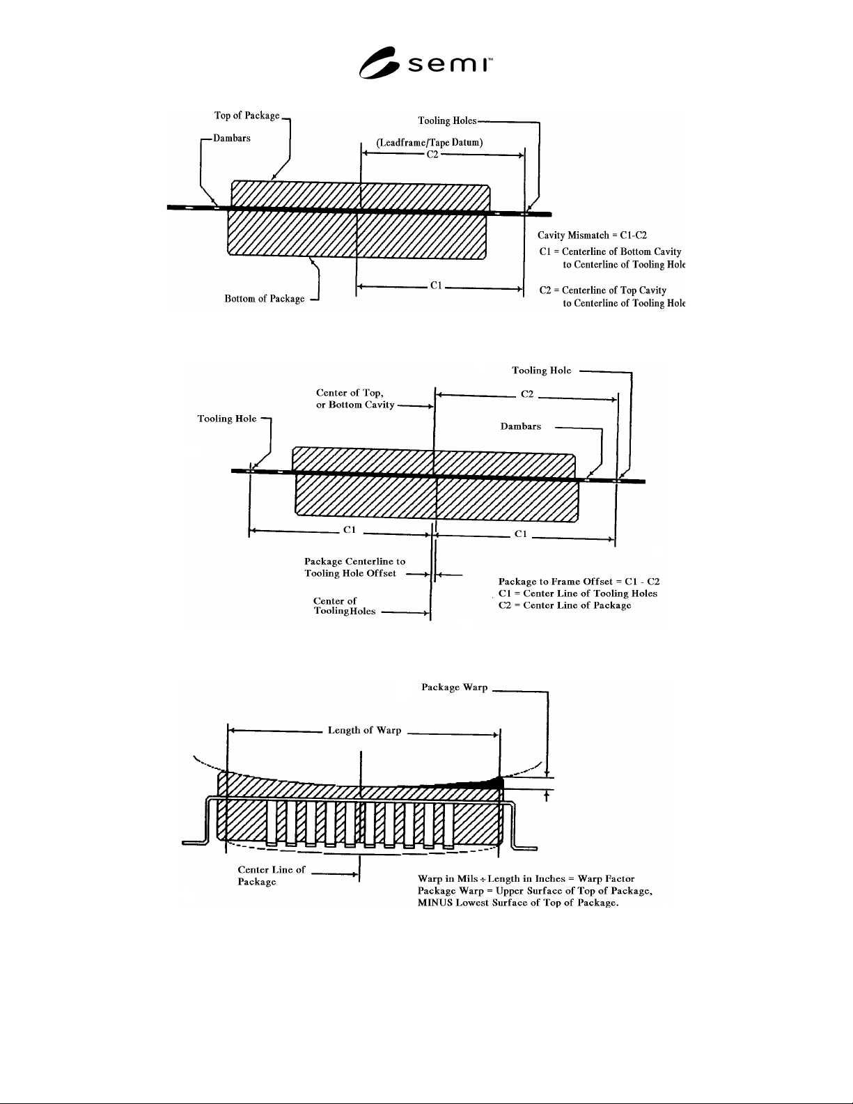
Figure 1
Top to Bottom Cavity Mismatch
Figure 2
Cavity to Frame Offset
Figure 3
Package Warpage
SEMI G36-88 © SEMI 1986, 1988 4
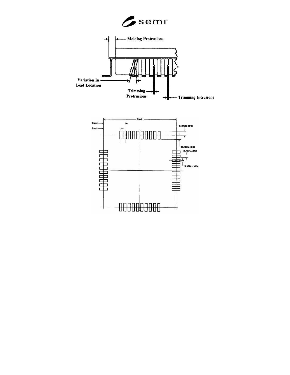
Figure 4
Parting Line Protrusion/Intrusion and Variation in Lead Location
Figure 5
Lead Position Overlay Example
NOTICE: These standards do not purport to address safety issues, if any, associated with their use. It is the
responsibility of the user of these standards to establish appropriate safety and health practices and determine the
applicability of regulatory limitations prior to use. SEMI makes no warranties or representations as to the suitability
of the standards set forth herein for any particular application. The determination of the suitability of the standard is
solely the responsibility of the user. Users are cautioned to refer to manufacturer’s instructions, product labels,
product data sheets, and other relevant literature respecting any materials mentioned herein. These standards are
subject to change without notice.
The user’s attention is called to the possibility that compliance with this standard may require use of copyrighted
material or of an invention covered by patent rights. By publication of this standard, SEMI takes no position
respecting the validity of any patent rights or copyrights asserted in connection with any item mentioned in this
standard. Users of this standard are expressly advised that determination of any such patent rights or copyrights, and
the risk of infringement of such rights, are entirely their own responsibility.
Copyright by SEMI® (Semiconductor Equipment and Materials
International), 3081 Zanker Road, San Jose, CA 95134. Reproduction o
f
the contents in whole or in part is forbidden without express written
consent of SEMI.

SEMI G37-88 © SEMI 1986, 19881
SEMI G37-88
SPECIFICATION FOR DIMENSIONS AND TOLERANCES USED TO
MANUFACTURE PLASTIC MOLDED SMALL OUTLINE PACKAGE
TOOLING
1 Preface
This document is a guideline for the ordering of tooling
required to mold and form plastic molded small outline
semiconductor packages. It is to be used by packaging
engineers, mold manufacturers, and end-of-line
toolmakers as the basis for defining the limits of
manufacturing tolerances.
2 Applicable Documents
2.1 ANSI Specification
1
Y14.5 — Dimensioning and Tolerancing
2.2 JEDEC Specification
2
Pub. No. 95 — Registered and Standard Outline for
Semiconductor Devices
2.3 Military Specification
3
MIL-STD-100 — Engineering Drawing Practices
3 Selected Definitions — Pr oduct Criteria
Tolerance Limits
mismatch and offset — defined with respect to package
only. As this family of packages has four sides, all
statements will be equally applicable in two (2) axes.
All mismatch and offset measurements are made after
molding and prior to trimming.
cavity to frame offset — will be measured prior to any
trimming operation. Offset will be defined as the
difference in bottom cavity position with respect to a
leadframe datum. The offset measurement will exclude
leadframe tolerances (see Figure 1).
top to bottom cavity mismatch — characterized by the
fact that the top and bottom cavities in the mold are not
aligned properly, causing a mismatch condition. The
measurement shall be stated as the difference in the
package top cavity position relative to the bottom cavity
position (see Figure 2).
parting line protrusions — those plastic excesses which
remain as a normal characteristic after normal molding,
deflashing, trimming, and singulation (see Figure 3).
1 ANSI, 1430 Broadway, New York, NY 10018
2 JEDEC, 20001 Eye Street, N.W., Washington, D.C. 20006
3 Military Standards, Naval Publications and Form Center, 5801
Tabor Avenue, PA 19120
top or bottom protrusions — those plastic excesses
(includes ejector pin crowns), which remain as a normal
characteristic extending from the smooth surface of the
molded package.
variations in lead location — defined with respect to a
90° angle from the top or bottom of the smooth surface
of the molded package as viewed on the end or side
projections (see Figure 3).
lead shoulder intrusions and protrusions — any
variations in straightness along the defined shoulder
essentially caused by dambar removal (see Figure 3).
package warpage — any non-linear dimensional
change from the mold cavity characteristic, usually
caused by incorrect package design or molding
practices (see Figure 4).
shoulder bend location — measured from the outermost
point of the shoulder bend radius (see Figure 5).
lead co-planarity — defined as the vertical lead
position with respect to a reference plane measured
after forming. The reference plane is defined by the
three lowest leads from the bottom of the package (see
Figure 6).
4 Ordering Information
4.1 Purchase orders for tooling for plastic molded high
density TAB semiconductor packages furnished to this
specification shall include the following items:
1. A package tooling outline drawing showing all
required dimensions listed in Section 5. Package
surface finish to be included.
2. A list of any tolerance limits which differ from
those in Section 6.
3. The type of tooling steel required.
4. The type of leadframe material and temper to be
used.
5. The type of plastic to be molded (if proprietary, a
statement of its shrinkage characteristics).
6. Sampling plan for compliance to Section 7.
7. The number of spare parts or expendable parts
desired.