semi合集-English.pdf - 第7532页
SEMI MF1771-0304 © SEMI 2003, 2004 9 11 Report 11.1 Report the following for each wafer, as appropriate for th e test conditions and as ag reed upon by the parties to the test: 11.1.1 Test Description : 11.1.1.1 Date, 11…
SEMI MF1771-0304 © SEMI 2003, 2004 8
()
()
()( )()
−−−
−
−
51
5
1
absln
abs
nVnV
nI
nI
(5)
while the new slope is computed from the last two
points,
()
()
() ( )()
−−
−
1
1
absln
abs
nVnV
nI
nI
(6)
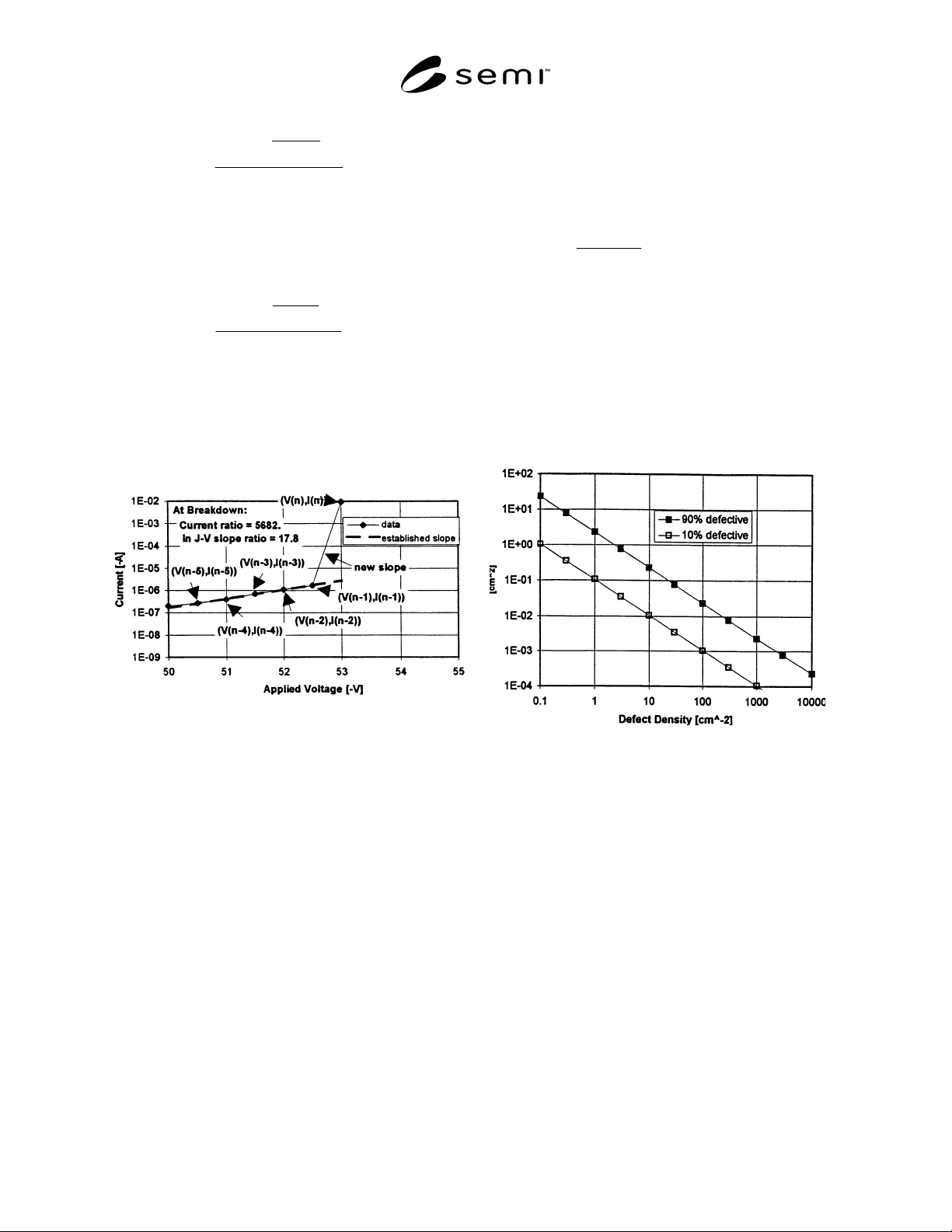
10.4.4 Testing for the failure criterion is done by taking
the ratio of Equation 6 to Equation 5. As can be seen
from Figure 3, this failure would be identified by failure
criteria Sections 9.9.2 and 9.9.3, as well as the slope
criterion Section 9.9.5.
Figure 3
Calculation of In J-V Slope Ratio Failure
Criterion for a p-Type Sample with 50-nm Gate
Oxide
10.5 Defect Density — To calculate a defect density, a
minimum criterion must be chosen by either the user or
negotiated with the user' s customer. This criterion can
take the form of a minimum breakdown voltage or
electric field strength, or a discontinuity in the
breakdown voltage distribution of the sample. Given
the fraction of devices reaching this criterion, the defect
density calculation may be based on a Poisson
relationship (see Standard 35) using the following
equation:
)exp( ADY −= (7)
where:
Y = yield of good units in terms of the defined
failure criterion,
A = area of sample, cm
2
, and
D = defect density, defects/cm
2
.
NOTE 4: Example: Given a total of 100 devices tested with
87 devices passing the minimum criterion for success and a
gate area of 0.08 cm
2
, the defect density would be as follows:
2
defects/cm7.1
08.0
)100/87ln(
==D
(8)
10.5.1 An undefined condition results if the number of
successes is zero. It may be necessary to change the
area of the test capacitor chosen for testing in order to
resolve meaningful defect densities. Figure 4 shows the
relationship between defect density and test capacitor
area required for resolution in terms of a minimum of
10% good or defective units in the sample.
NOTE 5: For example, a test capacitor with an area of 0.1
cm
2
can resolve defect densities between 1 and 25
defects/cm
2
, with 10 and 90% defective samples.
Figure 4
Test Capacitor Area Required to Resolve Various
Oxide Defect Densities, Assuming Poisson Statistics
10.6 Weibull Distributions — To convert cumulative
percentages to Weibull format (sometimes referred to
as “smallest extreme value probability distribution III”),
use the following equation:
(
)
)1ln(ln F
−
−
(9)
where ln is the natural log operator and F is the fraction
of accumulated failures. Care should be taken so that F
is never exactly 1 since this results in an undefined
situation.
SEMI MF1771-0304 © SEMI 2003, 2004 9
11 Report
11.1 Report the following for each wafer, as
appropriate for the test conditions and as agreed upon
by the parties to the test:
11.1.1 Test Description:
11.1.1.1 Date,
11.1.1.2 Time,
11.1.1.3 Operator,
11.1.1.4 Instrument station identity (if any),
11.1.1.5 Test temperature, and
11.1.1.6 Total number of devices tested.
11.1.2 Sample Description:
11.1.2.1 Average oxide thickness,
11.1.2.2 Gate area, cm
2
,
11.1.2.3 Gate material,
11.1.2.4 Oxide type (example thermal versus
deposited),
11.1.2.5 Structure type,
11.1.2.6 Conductivity type (n or p),
11.1.2.7 Bias mode (accumulation or depletion), and
11.1.2.8 Average computed series resistance (R
s
), if
performed.
11.1.3 Test Results:
11.1.3.1 Medians and means for the hard and soft
breakdown voltage distributions (V
BD
) and the current
densities at breakdown (J
BD
),
11.1.3.2 Histograms of the hard and soft breakdown
voltage and breakdown current density data. These
results may also be presented in Weibull plot format,
11.1.3.3 Percentage of devices falling into each failure
mode category by hard or soft failure voltage, or by
oxide electric field. Include results of the post-test for
each category, and
11.1.3.4 Defect densities computed as described in
Section 10.5, and as agreed upon by participating
parties.
NOTE 6: For homogenous groups, data can be combined for
the purposes of comparison.
12 Precision and Bias
12.1 At this time, precision has not been established. A
reproducibility test for the similar Standard 35 has been
reported.
5
13 Keywords
13.1 current density; defect density; electric field
strength; extrinsic breakdown; intrinsic breakdown;
oxide breakdown
5 Suehle, John S., “Reproducibility of JEDEC Standard Current and
Voltage Ramp Test Procedures for Thin-Dielectric Breakdown
Characterization,” Final Report, IEEE International Integrated
Reliability Workshop (IRW), IEEE Electron Devices Society, 1993,
pp. 22–34.
SEMI MF1771-0304 © SEMI 2003, 2004 10
RELATED INFORMATION 1
BACKGROUND OF METHOD
NOTICE: This related information is not an official part of SEMI MF1771. It was developed during the original
development of the document. This related information was approved for publication by full letter ballot on
December 4, 2003.
R1-1 Overview
R1-1.1 This is a voltage ramp test. It is most useful in
determining changes in a given process. It is intended
to be applied to arrays of similar capacitors on a silicon
wafer or group of wafers representing a process
condition specified by the user.
R1-2 Voltage Ramp
R1-2.1 While this test can, and might best be done
using a true linear voltage ramp, constraints of the
automated test equipment most often used in its
performance lead to widespread use of a staircase of
voltage steps to simulate the ramp. The ramp rate is
specified in terms of the rate of increase of the oxide
electric field. For oxides thicker than about 20 nm, the
oxide electric field has been commonly estimated by
dividing the applied voltage by the oxide thickness, but
for thinner films, significant errors may be introduced
by ignoring the effects of non-zero flat band voltage of
the MOS capacitor and voltages developed across the
silicon substrate (and the gate electrode as well, if it is
polysilicon) due to band bending and series resistance.
One approach to estimation of the relationship between
sample parameters and oxide field strength is found in
Section 10.2.
R1-3 Current Sampling
R1-3.1 In order to provide adequate breakdown field
strength resolution, it is specified that current readings
be taken after a maximum electric field change of 0.1
MV/cm. Taken together with the specified voltage
ramp rate, this leads to a maximum time between
current readings of 100 ms. In the case in which the
test is done using a voltage staircase, this implies use of
a 100-ms voltage step duration, with one current
reading taken at each step.
R1-4 Failure Criteria
R1-4.1 Both “hard” and “soft” failure criteria are
provided for in this test methods.
R1-4.2 Techniques for detection of hard oxide failure
for thin dielectrics may require high resolution, low
noise current-voltage data. For this reason, hard failure
criteria are defined in two measurement regimes, one
below and one above a threshold current level where
noise is reduced. This current level is commonly in the
range 1 nA to 0.1 µA for most test systems. Hard
failure criteria below the noise threshold level are
defined as follows:
R1-4.2.1 Current greater than or equal to 0.98 times
the compliance limit of the current score — This
condition signals total collapse of the capacitor.
R1-4.2.2 Current change by a factor of 1000 in a
single voltage step — Units with gross defects failing at
low voltages where currents are below the noise
threshold commonly fail with very large increases in
current.
R1-4.2.3 Consecutive current increases by a factor of
10 in each of two voltage steps — Test capacitors that
are initially highly conductive, as from a pinhole, often
do not display destructive breakdown, but rather show
steeply rising diodic leakage currents. This failure
criterion is designed to identify these defective units at
low voltage. Above the noise threshold current level,
the two criteria above remain in force, and two others
are added, as follows:
R1-4.2.4 Current change by a factor of 10 in a single
step — In the Fowler-Nordheim regime, current
changes are much less than this value for the small
increment in oxide field associated with a single voltage
step.
R1-4.2.5 Change in the logarithmic slope of the J-V
curve by a factor of 3 — This criterion becomes of
increasingly great value for oxide films thinner than 10
nm, where destructive breakdown is often accompanied
by very small changes in current, because of the very
low resistance of these oxides at very high fields (see
Standard 35-2).
R1-4.3 Another parameter associated with hard failure
is the hard failure current density, defined as the value
of the current at the last measurement point prior to
detection of hard failure, divided by the area of the
capacitor.
R1-4.4 Soft failures are associated with the passage of
a predetermined current through the capacitor under
test. This type of criterion has been traditionally used,
since in the past, passage of any measurable current
through an oxide was normally associated with hard
failure. More recently, where oxides have commonly
been capable of sustaining Fowler-Nordheim tunneling
conduction, use of such a criterion yields results
indicative of the uniformity of the samples being tested.