semi合集-English.pdf - 第7355页
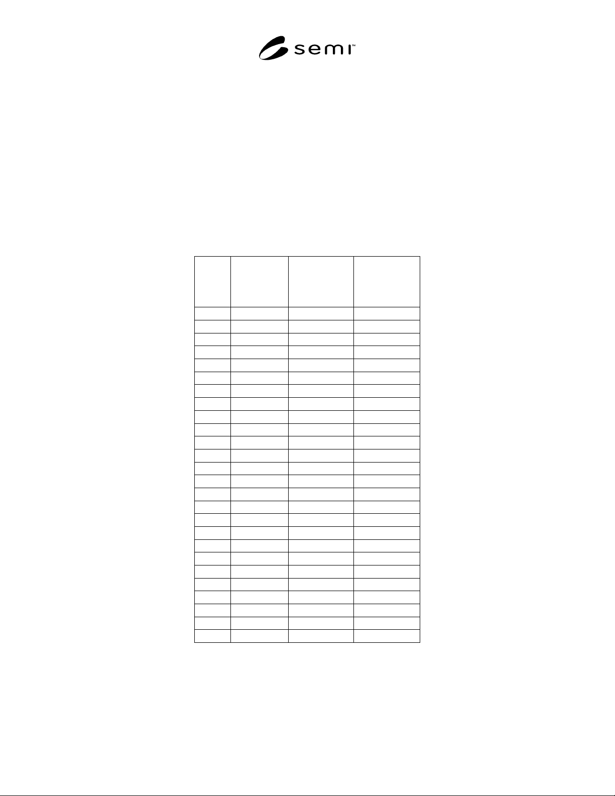
SEMI MF1391-0704 © 2004 7 13 Precision 13.1 A round robin was carri ed out by JEI DA (now JEITA 1 ). The results o f this 21-l aboratory study are shown in Table 1. Figur e 2 shows that the sample standard de viation i n…

SEMI MF1391-0704 © 2004
6
6
10.6 For measurements at room temperature, locate the
wavenumber corresponding to the maximum
absorbance in the region from 603 to 607 cm
−1
. For
measurements at cryogenic temperatures (below 80 K),
locate the wavenumber corresponding to the maximum
absorbance in the region from 605 to 609 cm
−1
.
10.6.1 Record the value of that wavenumber, to four
significant figures, as W
p
. Record the maximum
absorbance as A
p
, the absorbance of the absorption
peak.
10.6.2 Record the baseline absorbances, A
b
, as the
value of the baseline defined in 10.5 at W
p
.
10.6.3 Record both A
p
and A
b
to three significant
figures.
10.7 Determine and record the full width at half
maximum (FWHM) of the peak. If the FWHM of the
peak is greater than 6 cm
−1
(room temperature) or 3
cm
−1
(cryogenic temperatures), the spectrum was not
properly obtained, and the instrument needs further
adjustment, or the specimen is under stress. See
Section 3.4 for a list of factors that influence FWHM.
Adjust the instrument in order to achieve the proper
FWHM and repeat the procedure.
10.8 Record the apodization function and the number of
zero-fills used (FT-IR instruments) or the spectral slit
width for dispersive infrared (DIR) instruments.
11 Calculation
11.1 Calculate the absorption coefficient, α, using the
expression:
)(
03.23
bp
AA
X
−=α (1)
where:
X = test specimen thickness, mm,
A
p
= the peak value of the carbon-only absorbance
spectrum, and
A
b
= the baseline value of the carbon-only absorbance
spectrum.
NOTE 4: This equation does not include a correction factor
for multiple reflections. Such a correction factor is not neces-
sary, due to the very strong lattice absorption at 610 cm
−1
.
11.2 For measurements at room temperature, calculate
the substitutional carbon content in atoms/cm
3
or parts
per million atomic (ppma) as follows:
6
6 Inoue, N., Stso. T. Nozaki, T., Endo, K., and Mizauma, K., “High
Reliability Infrared Measurement of Oxygen and Carbon in Silicon,”
in Emerging Semiconductor Technology, ASTM STP 960, D. C.
Gupta and P. H. Langer, eds., (ASTM, Philadelphia, 1987), pp. 365–
377.
ppma64.1
atoms/cm102.8ContentCarbon
316
α=
α×=
(2)
11.3 For measurements at cryogenic temperature,
calculate the content of substitutional carbon in
atoms/cm
3
or ppma as follows:
ppma74.0
atoms/cm107.3ContentCarbon
316
α=
α×=
(3)
NOTE 5: The calibration factor used in this test method was
determined as result of a study carried out in Japan by the
Silicon Technologies Committee of the Japanese Electronic
Industries Development Association (JEIDA), now JEITA,
1
in
the mid-1980’s. Further data analysis to eliminate recognized
systematic error was carried out by the ASTM subcommittee
assigned for this effort. The factor resulting from this study
has an uncertainty of ± 0.4 × 10
16
atoms/cm
2
or ±0.08
ppma·cm for the room temperature measurements. The
calibration factor for cryogenic measurements was calculated
using the ratio given in Kolbesen and Mladcnović.
7
The
uncertainty of the cryogenic temperature factor is therefore
± 0.2 × 10
16
atoms/cm
2
or ± 0.04 ppma·cm.
12 Report
12.1 Report the following information:
12.1.1 The instrument used, the operator, and the date
of the measurements,
12.1.2 Identification of test and reference specimens,
12.1.3 For room temperature measurements, the
nominal temperature of the sample chamber. For
cryogenic measurements, the nominal temperature of
the sample holder,
12.1.4 Thickness of test and reference specimen,
12.1.5 Location and size of the illuminated area on the
specimen,
12.1.6 For FT-IR instruments: (a) the apodization
function used, (b) the amount of zero-filling, and (c) the
number of data/cm
−1
. For dispersive instruments: (a)
the scan time/cm
−1
, (b) the spectral slit width, and (c)
the resolution at 600 cm
−1
,
12.1.7 Spectral full width at half maximum of the
absorption peak,
12.1.8 W
p
, wavenumber in cm
−1
of the absorption peak,
12.1.9 The absorption coefficient due to substitutional
carbon, α, in cm
−1
,
12.1.10 Carbon concentration, in ppma or in
atoms/cm
3
, and
12.1.11 The conversion coefficient used.
7 Kolbesen, B. O., and Mladcnović, T., Kristall und Technik 15(1),
K1–K3 (1980).
SEMI MF1391-0704 © 2004 7
13 Precision
13.1 A round robin was carried out by JEIDA (now
JEITA
1
). The results of this 21-laboratory study are
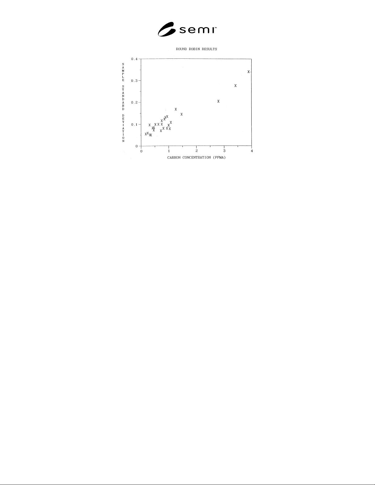
shown in Table 1. Figure 2 shows that the sample
standard deviation increases with concentration value.
13.2 A single-laboratory investigation of the precision
of carbon measurement at cryogenic temperature with a
Fourier transform spectrophotometer was conducted
using a single sample analyzed once a day over a 30-
day period (30 measurement values). From this single-
laboratory, multiple-operator, multiple-day, single-
sample investigation of precision of carbon
measurement, the precision was found to be 0.02 ppma
(2 standard deviations). Nominal carbon content of the
sample was 0.16 ppma.
14 Bias
14.1 The bias of this test method cannot be evaluated
because there are no available reference standards
suitable for evaluating bias.
15 Keywords
15.1 carbon; infrared absorption; infrared spectroscopy;
silicon; single crystal silicon
Table 1 JEIDA Round Robin Results
Sample
Number
Number of
Measurements
Mean Value of
Concentration o
f
Substitutional
Carbon
Sample Standard
Deviation
1 21 2.79 0.204
2 21 3.89 0.342
3 21 0.23 0.059
4 21 0.35 0.050
5 21 0.74 0.100
6 21 0.93 0.081
7 21 1.03 0.079
8 21 1.25 0.168
9 21 0.41 0.083
10 21 0.84 0.123
11 20 0.80 0.081
12 20 0.94 0.135
13 20 0.99 0.095
14 20 0.30 0.097
15 20 0.46 0.084
16 20 0.71 0.070
17 20 1.07 0.108
18 20 1.46 0.145
19 20 3.41 0.276
20 20 0.31 0.051
21 20 0.45 0.073
22 20 0.51 0.099
23 20 0.74 0.116
24 20 0.16 0.055
25 20 0.62 0.100
26 20 0.87 0.131
SEMI MF1391-0704 © 2004
8
8
Figure 2
Round Robin Results
NOTICE: SEMI makes no warranties or representations as to the suitability of the standards set forth
herein for any particular application. The determination of the suitability of the standard is solely the
responsibility of the user. Users are cautioned to refer to manufacturer's instructions, product labels,
product data sheets, and other relevant literature, respecting any materials or equipment mentioned
herein. These standards are subject to change without notice.
By publication of this standard, Semiconductor Equipment and Materials International (SEMI) takes no
position respecting the validity of any patent rights or copyrights asserted in connection with any items
mentioned in this standard. Users of this standard are expressly advised that determination of any such
patent rights or copyrights, and the risk of infringement of such rights are entirely their own
responsibility.
Copyright by SEMI® (Semiconductor Equipment and Materials
International), 3081 Zanker Road, San Jose, CA 95134. Reproduction o
f
the contents in whole or in part is forbidden without express written
consent of SEMI.