semi合集-English.pdf - 第2875页
SEMI E105-0701 © SEMI 2000, 2001 26 5. Factory Operation dose n ot use the following interfaces def i ned in section 6.1.6. (*1) • whatNextForMaterialGroupByCount • whatNe xtFor Dur ableB yCount R3-2 Simulator Based Sche…
SEMI E105-0701 © SEMI 2000, 200125
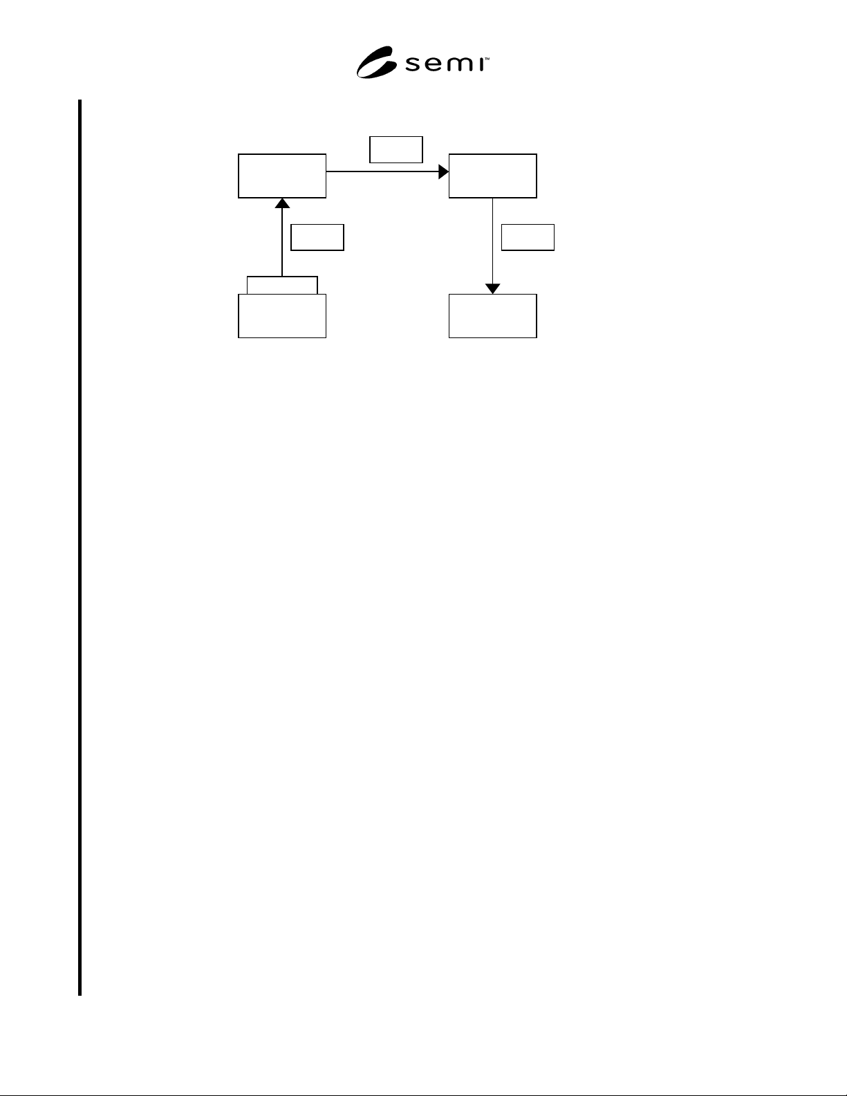
R3-1.2 Case 1 – Factory Operation decides storage machine (Refer to Scenarios R2-3 and R2-4)
Stocker 1
Production
Eq. 1
Stocker 2
Production
Eq. 2
Operation 1000 Operation 2000
Carrier A
AGV 1 OHT 1
OHS 2
Figure R3-2
1. Carrier A processing on Eq.1 (Operation 1000) is finished.
2. Next operation for Carrier A is “2000” and the production equipment in operation “2000”is Eq.2 only.
3. Factory Operation makes the logistic decision .
(1) Transfer Carrier A from Eq.1 to Eq.2
or
(2) Transfer Carrier A from Eq.1 to Stocker 2.
4. Factory Operation uses the following interfaces defined in section 6.1.6. (*1)
• whatNextForResourceByCount
• whatNextForMaterialGroupByCount
• whatNextForDurableByCount
5. Factory Operation dose not use the following interfaces defined in section 6.1.6. (*1)
• whereNextForMaterialGroup
• whereNextForDurable
6. Scheduler / Dispatcher shows the waiting Lot list in operation “2000” (Eq.2) to Factory Operation
R3-1.2 Case 2 – Scheduler / Dispatcher decides storage machine (Refer to Scenarios R2-5 and R2-6)
1. Carrier A processing on Eq.1 (Operation 1000) is finished.
2. Next operation for Carrier A is “2000” and the production equipment in operation “2000”is Eq.2 only.
3. Scheduler / Dispatcher checks the port status of Eq.2 and makes the logistic decision .
(1) Transfer Carrier A from Eq.1 to Eq.2
or
(2) Transfer Carrier A from Eq.1 to Stocker 2.
4. Factory Operation uses the following interfaces defined in section 6.1.6. (*1)
• whatNextForResourceByCount
• whereNextForMaterialGroup
• whereNextForDurable
SEMI E105-0701 © SEMI 2000, 2001 26
5. Factory Operation dose not use the following interfaces defined in section 6.1.6. (*1)
• whatNextForMaterialGroupByCount
• whatNextForDurableByCount
R3-2 Simulator Based Scheduler/Dispatcher (Refer to Scenarios R2-1 and R2-2)
R3-2.1 Basic Functions
Simulator Based Scheduler / Dispatcher has a forecast list for each production equipment and provides the lot list
with forecast time stamp to Factory Operation.
Factory Operation uses “forecastFor…” interfaces defined in section 6.1.6. (*1)
EQ-1 (Operation 1000)
09:00 - 10:00 Lot-1
10:00 - 11:00 Lot-2
11:00 - 12:00 NPW-1
12:00 - 13:00 Maintenance
EQ-2 (Operation 1000)
09:00 - 10:00 NPW-2
10:00 - 11:00 Lot-3
11:00 - 12:00 Maintenance
12:00 - 13:00 Lot-4
Simulator Based S/D output
Figure R3-3
Remarks
In (*1), the conformance of each interfaces to each case of Scheduler/Dispatcher are described. These are only for
reference and are not the requirement to the Scheduler/Dispatcher product. For example, Simulator Based
Scheduler / Dispatcher may support “whatNextFor…” interfaces.
NOTICE: SEMI makes no warranties or representations as to the suitability of the standard set forth herein for any
particular application. The determination of the suitability of the standard is solely the responsibility of the user.
Users are cautioned to refer to manufacturer’s instructions, product labels, product data sheets, and other relevant
literature respecting any materials mentioned herein. These standards are subject to change without notice.
The user’s attention is called to the possibility that compliance with this standard may require use of copyrighted
material or of an invention covered by patent rights. By publication of this standard, SEMI takes no position
respecting the validity of any patent rights or copyrights asserted in connection with any item mentioned in this
standard. Users of this standard are expressly advised that determination of any such patent rights or copyrights, and
the risk of infringement of such rights, are entirely their own responsibility.
Copyright by SEMI® (Semiconductor Equipment and Materials
International), 3081 Zanker Road, San Jose, CA 95134. Reproduction o
f
the contents in whole or in part is forbidden without express written
consent of SEMI.

SEMI E107-1102 © SEMI 2001, 2002 1
SEMI E107-1102
SPECIFICATION OF ELECTRIC FAILURE LINK DATA FORMAT FOR
YIELD MANAGEMENT SYSTEM
This specification was technically approved by the Global Information & Control Committee and is the direct
responsibility of the Japanese Information & Control Committee. Current edition approved by the Japanese
Regional Standards Committee on July 19, 2002. Initially available at www.semi.org October 2002; to be
published November 2002. Originally published March 2001; previously published November 2001.
1 Purpose
1.1 The objective of this document is standardization
of the specific data format passed from the test
equipment to the Yield Management System. The Yield
Management System is a kind of data server for detail
test data and geometrical defect data of patterns on a
wafer as described in the Terminology section of this
document.
1.2 This document assumes a Yield Management
System in which test equipment electrical failure
information is managed and analyzed in an integrated
manner. Examples of test equipment failure information
include bit map data, bin data, and inpsection
information obtained by devices such as wafer
inspection equipment and review tools. Standardization
of the data file format helps to reduce the development
burden on customers and related vendors.
2 Scope
2.1 This document specifies the data file format for
transferring from test equipment to a Yield
Management System.
2.2 This document is an extension of the general map
data item standard, i.e. SEMI G81, and the general map
data format document, currently under development.
This document does not redefine the general
specification.
2.3 The scope of this document is just defining data
items and their formats. Data file creation methods,
data creating environments and file naming conventions
are outside of the scope of this document. Also,
communication protocols to transfer the data are
beyond the scope of this document.
2.4 This standard does not purport to address safety
issues, if any, associated with its use. It is the
responsibility of the user of this standard to establish
appropriate safety health practices and determine the
applicability or regulatory limitations prior to use.
3 Limitations
3.1 This standard defines extensional data for YMS
Link Data map for generic test data map standardized
by SEMI G81 and G85, data format of each item for
YMS Link Data is defined independently as extra
definition here.
4 Referenced Standards
4.1 SEMI Standards
SEMI E5 — SEMI Equipment Communication
Standard 2 Message Content (SECS-II)
SEMI E30.1 — Inspection and Review Specific
Equipment Model (ISEM)
SEMI G81 — Specification for Map Data Items
SEMI G85 — Specification for Map Data Format
NOTE 1: Unless otherwise indicated, all documents cited
shall be the latest published versions.
5 Terminology
5.1 Defintions
5.1.1 analog data — One of three categories of data:
measured values such as voltage or current obtained
when test equipment measures a semiconductor
device’s electrical characteristics, parameter values
which are test parameters when measuring, and limit
values which are decision parameters if test results are
pass or fail.
5.1.2 bin data — same as Category below.
5.1.3 category — data indicating the type of
electric
failure or rank of characteristics of die tested by the test
equipment. Used in the same manner as Bin Data in this
standard.
5.1.4 cell-logical-address — gives the electrical
location of a memory cell in a die.
5.1.5 cell-logical-io-number — number identifying the
IO data which can be simultaneously electrically
accessed within a memory device.
5.1.6 cell-physical-address — gives location of a
memory cell in a die on two-dimensional plane.
5.1.7 die — a unit equivalent to one die on a wafer.
Also known as Chip.