semi合集-English.pdf - 第7231页
SEMI MF154-0305 © SEMI 2003, 2005 5 Figure 16 Oxidat ion Induced Sta cking Faults on (100) Silicon Fo llowing Oxidation and 3-min Secco Etch, Magnificati on 200× Figure 17 Oxidat ion Induced Sta cking Faults on (111) Sil…
SEMI MF154-0305 © SEMI 2003, 2005 4
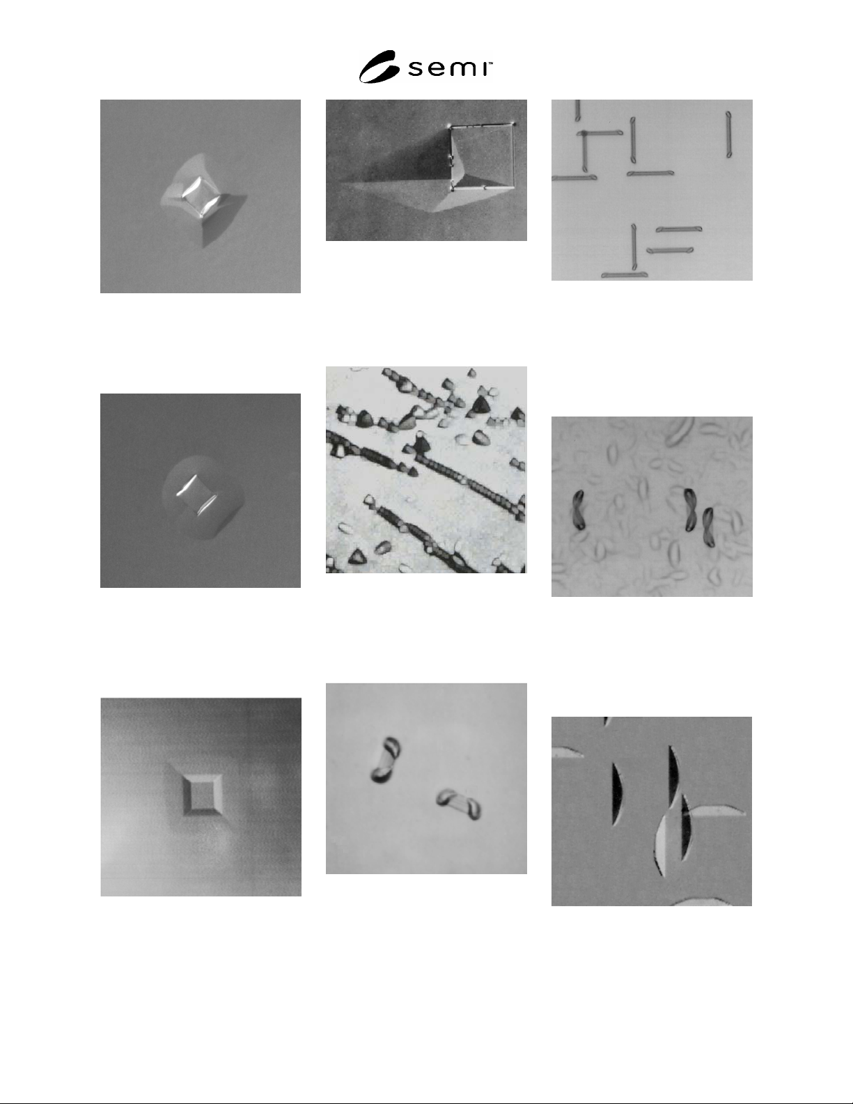
Figure 7
Epitaxial Stacking Faults on
(100), No Preparation Required,
Size Dependent Upon EPI
Thickness
Figure 8
Epitaxial Stacking Faults on
(100), No Preparation Required,
Size Dependent Upon EPI
Thickness
Figure 9
Epitaxial Growth Hillock on
(100), No Preparation Required,
Size Dependent Upon EPI
Thickness
Figure 10
Epitaxial Stacking Faults on
(100), No Preparation Required,
Size Dependent Upon EPI
Thickness
Figure 11
Lineage on (111) Silicon
Following Preferential Etch,
Magnification 140×
Figure 12
Oxidation Induced Stacking
Faults on (100) Silicon Following
Oxidation and 4-min Wright
Etch, Magnification 200×
Figure 13
Oxidation Induced Stacking
Faults from Liquid Hone
Damage on a (100) Silicon
Polished Frontside Surface
Following Oxidation at 1100°C
and 1-min Schimmel Etch,
Magnification 1500×
Figure 14
Oxidation Induced Stacking
Faults from Liquid Hone
Damage on a (100) Etched Back
Surface Following Oxidation at
1100°C and 1-Min Schimmel
Etch, Magnification 1500×
Figure 15
Oxidation Induced Stacking
Faults on (100) Silicon Following
Oxidation and 3-Min Secco Etch,
Magnification 500×
SEMI MF154-0305 © SEMI 2003, 2005 5
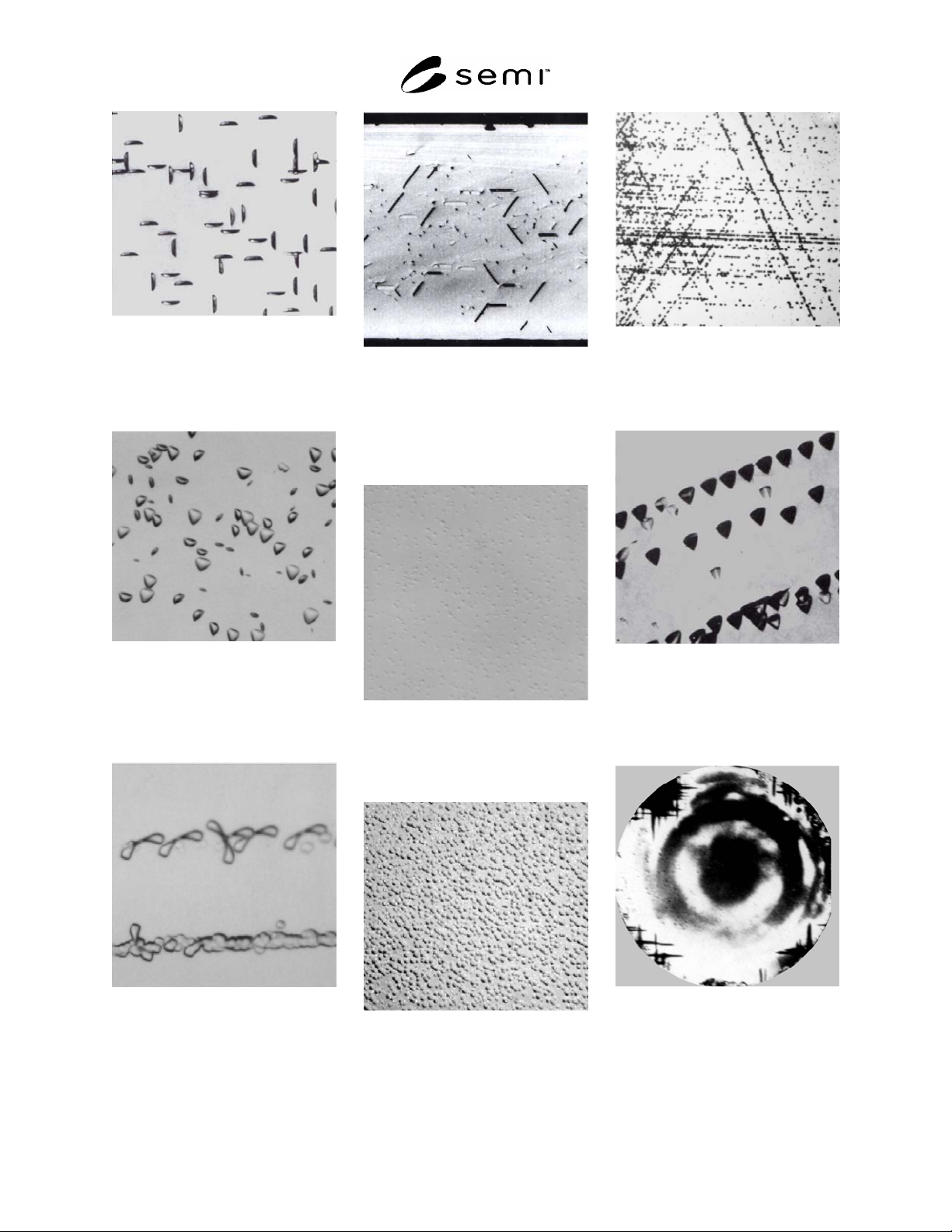
Figure 16
Oxidation Induced Stacking
Faults on (100) Silicon Following
Oxidation and 3-min Secco Etch,
Magnification 200×
Figure 17
Oxidation Induced Stacking
Faults on (111) Silicon Following
Oxidation and 4-min Wright
Etch, Magnification 200×
Figure 18
Oxidation Induced Stacking
Faults Caused by a Scratch on
(100) Silicon Following Oxidation
and 2-min Wright Etch,
Magnification 400×
Figure 19
Oxidation Induced Stacking
Faults and Precipitates Found on
the Cleavage Face of a Silicon
Wafer After Thermal Treatment
and 3-min Secco Etch,
Magnification 100×
Figure 20
Relatively Small Shallow Pits on
(111) Following Oxidation and
4-min Wright Etch,
Magnification 200×
Figure 21
Relatively Large Shallow Pits on
(111) Following Oxidation and
4-min Wright Etch,
Magnification 200×
Figure 22
Slip on a (111) Preferentially
Etched Wafer, Magnification 5×
Figure 23
Slip on a (111) Preferentially
Etched Wafer, Magnification
140×
Figure 24
Slip Lines on a (100) Wafer
Visible as a Cross Hatched
Pattern Near the Edge Because
Shallow Pits are Gettered
Following Oxidation and 4-min
Wright Etch
SEMI MF154-0305 © SEMI 2003, 2005 6
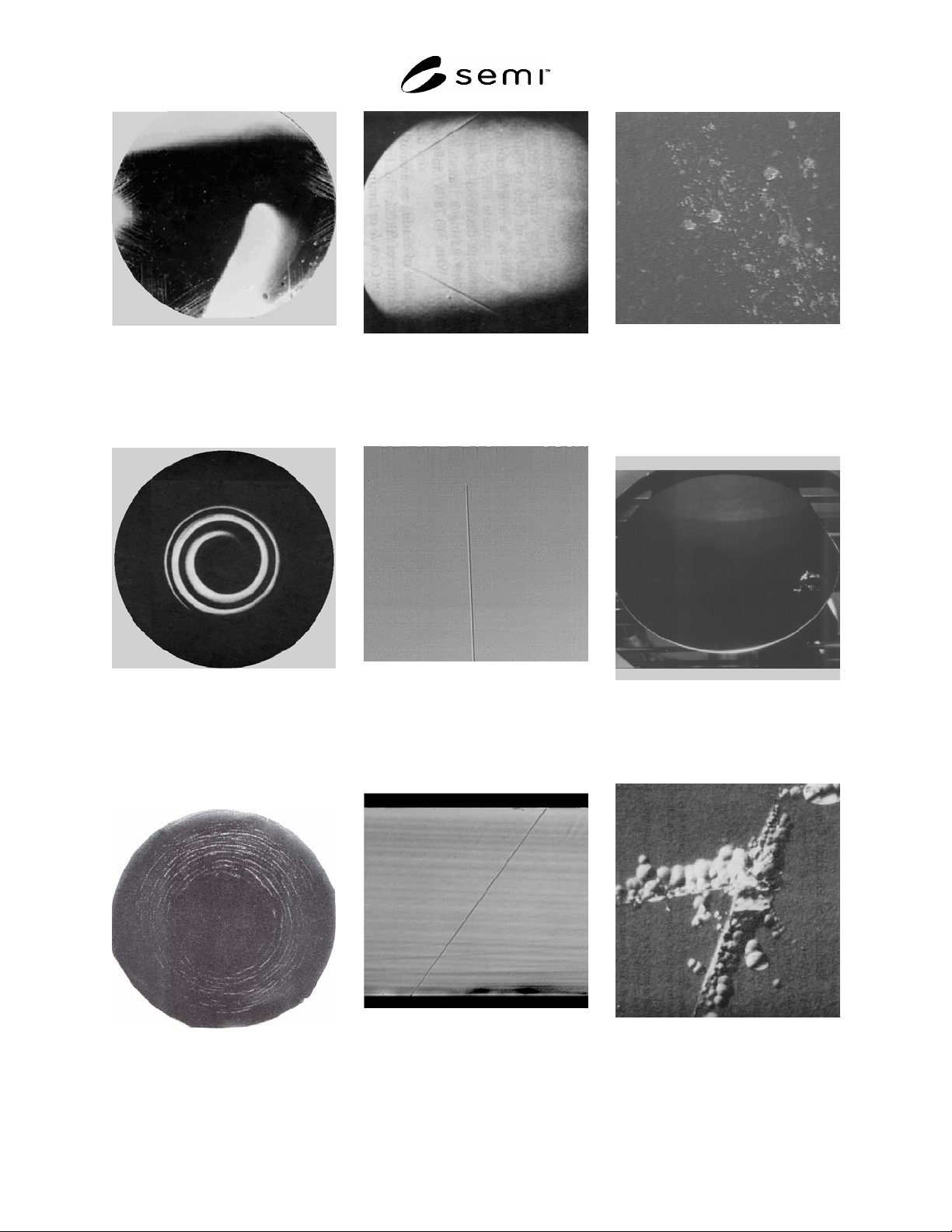
Figure 25
Slip on a (111) Wafer Following
10-min Wright Etch, Full Wafer
View
Figure 26
Swirl Pattern Developed by
Preferentially Etching a
Czochralski Grown
10 to 20
·cm
Lapped Silicon Wafer
Figure 27
A-swirl on As-grown Float-zone
Silicon Following Preferential
Etch, Full Wafer View
Figure 28
Twin Lines in a (111) Wafer after
Preferential Etching, Full Wafer
View
Figure 29
Twin Line Following 6.5
m
Epitaxial Deposition, No Other
Sample Preparation Required,
Magnification 300×
Figure 30
Twin Lamella in a <110> Cleaved
Vertical Cross Section Following
2.6
m Removal
in Leo (Modified Sirtl) Etch
Figure 31
Area Contamination,
Magnification 100×
Figure 32
Area Contamination Seen With a
High Intensity Light Source, Full
Wafer View
Figure 33
Crack, Resulting from the
Impact on the Wafer Surface,
Following Preferential Etch,
Magnification 450×