semi合集-English.pdf - 第6055页
SEMI G6-89 © SEMI 1 983, 199 6 1 SEMI G6-89 TEST METHOD FOR SEA L RING FL AT NESS 1 Purpose This specification covers t he method for determining the maxi mu m d evi atio n be tween t he sea l ri ng and a reference plan …
SEMI G5-87 © SEMI 1980, 1996 6
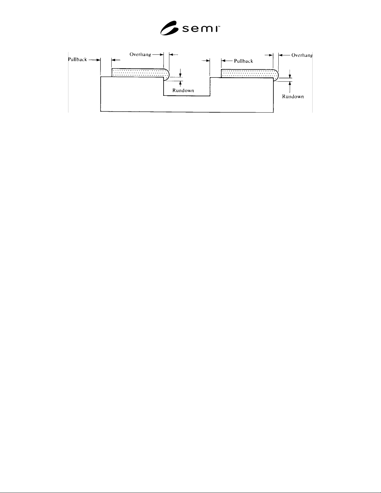
Figure 5
Glass Misalignment
NOTICE: These standards do not purport to address safety issues, if any, associated with their use. It is the
responsibility of the user of these standards to establish appropriate safety and health practices and determine the
applicability of regulatory limitations prior to use. SEMI makes no warranties or representations as to the suitability
of the standards set forth herein for any particular application. The determination of the suitability of the standard is
solely the responsibility of the user. Users are cautioned to refer to manufacturer’s instructions, product labels,
product data sheets, and other relevant literature respecting any materials mentioned herein. These standards are
subject to change without notice.
The user’s attention is called to the possibility that compliance with this standard may require use of copyrighted
material or of an invention covered by patent rights. By publication of this standard, SEMI takes no position
respecting the validity of any patent rights or copyrights asserted in connection with any item mentioned in this
standard. Users of this standard are expressly advised that determination of any such patent rights or copyrights, and
the risk of infringement of such rights, are entirely their own responsibility.
Copyright by SEMI® (Semiconductor Equipment and Materials
International), 3081 Zanker Road, San Jose, CA 95134. Reproduction o
f
the contents in whole or in part is forbidden without express written
consent of SEMI.
SEMI G6-89 © SEMI 1983, 19961
SEMI G6-89
TEST METHOD FOR SEAL RING FLATNESS
1 Purpose
This specification covers the method for determining
the maximum deviation between the seal ring and a
reference plane defined by three fixed points on the seal
ring. This method will not work on parts smaller than
0.330" × 0.330".
2 Equipment
2.1 Flat plate (black granite calibrated at ± 0.000025"
(± 0.000835 mm) or equivalent).
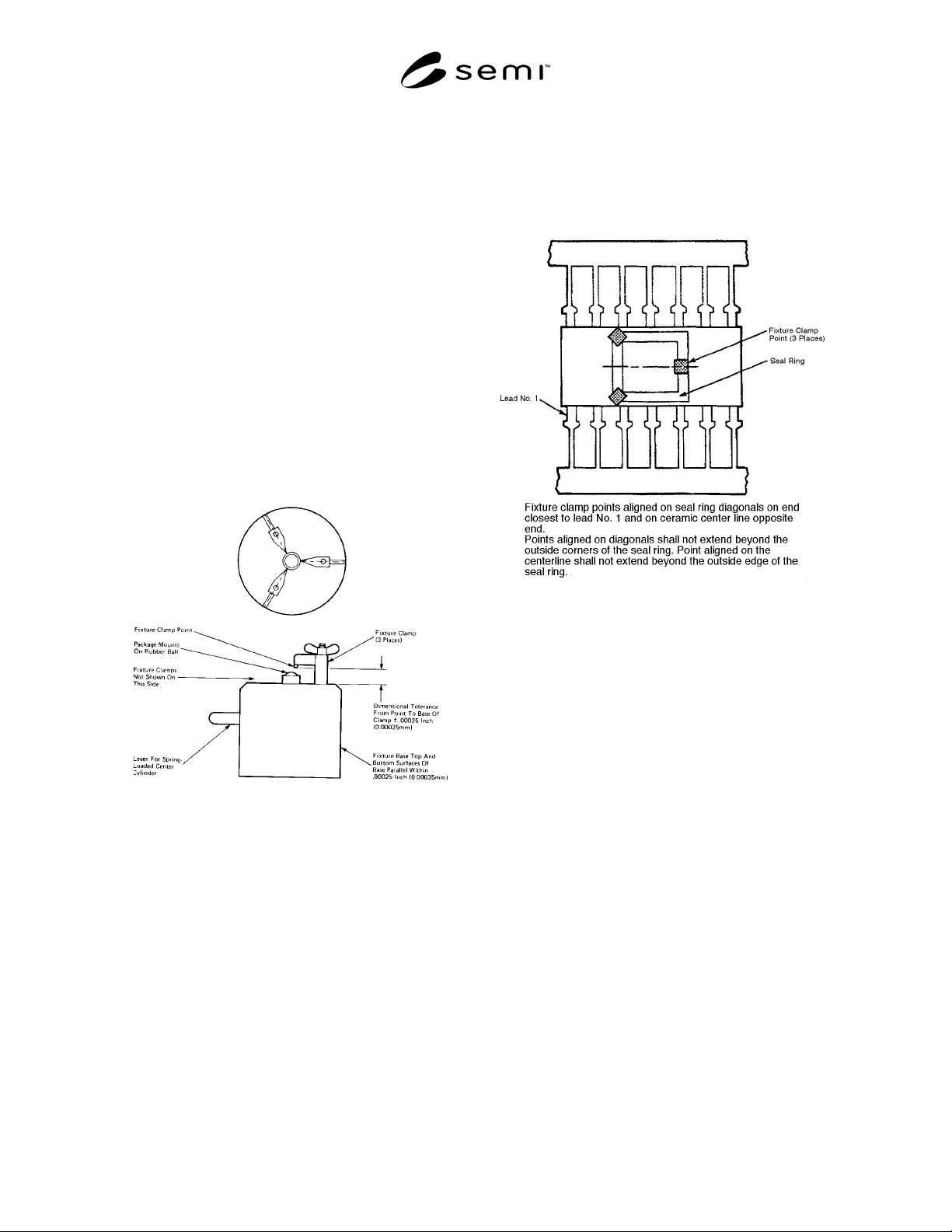
2.2 Fixture Clamps — Three required (See Figure 1).
2.3 Fixture Base — (See Figure 1).
2.4 Test Indicator — (Hamilton Kwik Check or
equivalent).
Figure 1
Fixture Base and Clamp Assembly
3 Preparation
3.1 Fixture clamps shall be adjusted for part to be
measured (see Figure 2).
3.2 The gaging fixture is to be calibrated with a
precision ground gage block before each sample is
measured.
3.2.1 Place gage block under the three fixture clamp
points and release center cylinder to hold in place.
3.2.2 Position fixture base so the point of the test
indicator is on the gage block.
3.2.3 Move fixture base so the point of the test
indicator traverses the entire surface of the gage block.
The total deviation read on the test indicator shall not
exceed 0.0005" (0.013 mm).
Figure 2
Fixture Clamp Orientation
4 Procedure
4.1 Place the package under the three fixture clamp
points and release cylinder to hold in place (see Figure
2) for orientation of package seal ring and fixture clamp
points.
4.2 Position fixture base so the point of the test
indicator is on the package seal ring.
4.3 Move fixture base so the point of the test indicator
traverses the length of the seal ring.
4.3.1 Move fixture base so the point of the test
indicator stays in the middle of the seal ring.
4.3.2 Test indicator shall be relocated twice to get
around fixture points.
5 Evaluation
If material buildup on the seal ring is visible with the
unaided eye, the part shall not be used for this
measurement.

SEMI G6-89 © SEMI 1983, 1996 2
NOTICE: These standards do not purport to address
safety issues, if any, associated with their use. It is the
responsibility of the user of these standards to establish
appropriate safety and health practices and determine
the applicability of regulatory limitations prior to use.
SEMI makes no warranties or representations as to the
suitability of the standards set forth herein for any
particular application. The determination of the
suitability of the standard is solely the responsibility of
the user. Users are cautioned to refer to manufacturer’s
instructions, product labels, product data sheets, and
other relevant literature respecting any materials
mentioned herein. These standards are subject to
change without notice.
The user’s attention is called to the possibility that
compliance with this standard may require use of
copyrighted material or of an invention covered by
patent rights. By publication of this standard, SEMI
takes no position respecting the validity of any patent
rights or copyrights asserted in connection with any
item mentioned in this standard. Users of this standard
are expressly advised that determination of any such
patent rights or copyrights, and the risk of infringement
of such rights, are entirely their own responsibility.
Copyright by SEMI® (Semiconductor Equipment and Materials
International), 3081 Zanker Road, San Jose, CA 95134. Reproduction o
f
the contents in whole or in part is forbidden without express written
consent of SEMI.