semi合集-English.pdf - 第3847页
SEMI F21-1102 © SEMI 1995, 2002 1 SEMI F21-1102 CLASSIFICATION OF AIRBORNE MOLECULAR CONTAMINANT LEVELS IN CLEAN ENVIRONMENTS This classification was technically approved b y the Global Facilities Comm ittee and is the d…
SEMI F20-0305 © SEMI 1995, 2005 10
Secondar
y
Electron Ima
g
e Mode
Backscatter Electron Image Mode
(
a
)
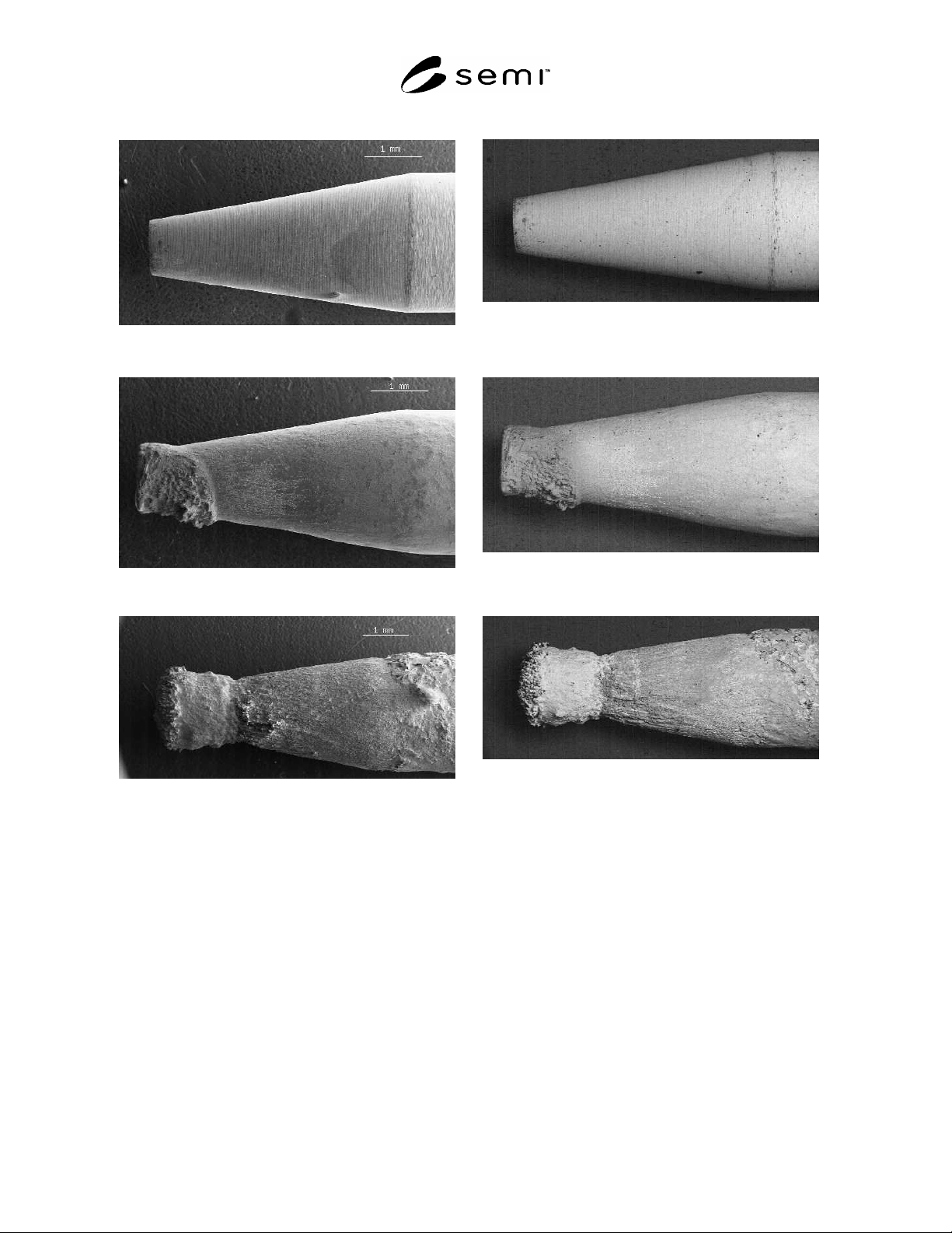
Electrode 1: 1 weld, 5 misfires.
(
b
)
Electrode 2: 1 weld, arc failed in level 3
(c)Electrode 3: 1 weld, arc failed in level 3; Changed shield gas to Ar, welded acceptably; Changed
back to Ar/H, 2 welds, then misfired.
Figure A2-2
Weldability: Effect of Copper Content and Shield Gas on Weld Electrodes
NOTICE: SEMI makes no warranties or representations as to the suitability of the standards set forth herein for any
particular application. The determination of the suitability of the standard is solely the responsibility of the user.
Users are cautioned to refer to manufacturer's instructions, product labels, product data sheets, and other relevant
literature, respecting any materials or equipment mentioned herein. These standards are subject to change without
notice.
By publication of this standard, Semiconductor Equipment and Materials International (SEMI) takes no position
respecting the validity of any patent rights or copyrights asserted in connection with any items mentioned in this
standard. Users of this standard are expressly advised that determination of any such patent rights or copyrights, and
the risk of infringement of such rights are entirely their own responsibility.
Copyright by SEMI® (Semiconductor Equipment and Materials
International), 3081 Zanker Road, San Jose, CA 95134. Reproduction of
the contents in whole or in part is forbidden without express written
consent of SEMI.
SEMI F21-1102 © SEMI 1995, 2002 1
SEMI F21-1102
CLASSIFICATION OF AIRBORNE MOLECULAR CONTAMINANT
LEVELS IN CLEAN ENVIRONMENTS
This classification was technically approved by the Global Facilities Committee and is the direct
responsibility of the North American Facilities Committee. Current edition approved by the North American
Regional Standards Committee on August 29, 2002. Initially available at www.semi.org September 2002; to
be published November 2002. Originally published in 1995.
1 Purpose
1.1 The purpose of this standard is to classify
microelectronics clean environments with respect to
their molecular (non-particulate) contaminant levels.
This standard classification provides a consistent means
of communicating acceptable contaminant levels of
groups of specific airborne molecular contaminants.
See Related Information 1 appended to this standard.
2 Scope
2.1 This standard classification is to be used in the
specification of semiconductor clean environments
(including process tool environments) and of
contamination control and measurement equipment
performance.
2.2 This standard does not purport to address safety
issues, if any, associated with its use. It is the
responsibility of the users of this standard to establish
appropriate safety health practices and determine the
applicability or regulatory limitations prior to use.
3 Referenced Standards
None.
4 Terminology
4.1 Definitions
4.1.1 acid — a corrosive material whose chemical
reaction characteristic is that of an electron acceptor.
4.1.2 base — a corrosive material whose chemical
reaction characteristic is that of an electron donor.
4.1.3 condensable — a substance (other than water),
typically having a boiling point above room
temperature at atmospheric pressure, capable of
condensation on a clean surface.
4.1.4 dopant — a chemical element which modifies the
electrical properties of a semiconductive material.
5 Basis of Classification
5.1 Classification is by the maximum allowable total
gas phase concentration of each category of material.
This classification system is depicted in Section 6. The
combination of a quantitative class for each of the four
categories yields a classification describing an
environment.
5.2 The maximum cumulative gas phase concentrations
of the four categories may be different.
5.3 Each category is designated by the letter “M,”
followed by the first letter of the category name A, B,
C, or D.
5.4 The integer following the category designator shall
indicate the maximum total gas phase concentration in
parts per trillion molar (pptm 1 ×10
-12
). For example, a
category MA-10 has a maximum allowable total
concentration of 10 parts per trillion molar for the
category of interest.
6 Classification
Material
Category
1* 10* 100* 1000* 10,000*
Acids MA-1 MA-10 MA-100 MA-1000 MA-10,000
Bases MB-1 MB-10 MB-100 MB-1000 MB-10,000
Condensables MC-1 MC-10 MC-100 MC-1000 MC-10,000
Dopants MD-1 MD-10 MD-100 MD-1000 MD-10,000
*Concentration, in parts per trillion
7 Reference Test Methods
7.1 Analytical methods capable of measuring the
classified levels at the agreed level of confidence shall
be used.
8 Related Documents
8.1 SEMI Standards
SEMI E45 — Test Method for the Determination of
Inorganic Contamination from Minienvironments Using
Vapor Phase Decomposition-Total Reflection X-Ray
Spectroscopy (VPD-TXRF), VPD-Atomic Absorption
Spectroscopy (VPD-AAS), or VPD/Inductively
Coupled Plasma-Mass Spectrometry (VPD/ICP-MS)
SEMI E46 — Test Method for the Determination of
Organic Contamination from Minienvironments Using
Ion Mobility Spectrometry (IMS)

SEMI F21-1102 © SEMI 1995, 2002 2
8.2 Other
8.2.1 Berro, N., Cook, J.P.D., et al., “Airborne
Contamination of Semiconductor Wafers Traced to
Humidification Plant Additives,” Journal of the IES,
pp. 15–18, November 1993.
8.2.2 Buchmann, K. and Rudolph, J., “Gas Chromato-
graphy of Radioactive Inorganic Compounds,” Journal
of Radiational Chemistry, 32(2): 245–64, 1976.
8.2.3 Dixon, W.J., “Processing Data for Outliers,”
Biometrics, 9(7): 74–89.
8.2.4 Kasi, S.R., Liehr, M., Thiry, P.A., et al.,
“Hydrocarbon Reaction with HF-Cleaned Si (100) and
Effects on Metal-Oxide-Semiconductor Device
Quality,” Applied Physics Letters, 59: 108–110, 1992.
8.2.5 Kelly, T.J. and Kinkead, D.A., “Testing of
Chemically Treated Adsorbent Air Purifiers,” ASHRAE
Journal, August 1993.
8.2.6 Kinkead, D.A., “Controlling a Killer: How to
Win the War Over Gaseous Contaminants,”
Cleanrooms, June 1993.
8.2.7 Kinkead, D.A. and Higley, J.K., “Targeting
Gaseous Contaminants in Wafer Fabs: Fugitive
Amines,” Microcontamination, pp. 37–40, June 1993.
8.2.8 Mori, E.J., Dowdy, J.D., and Shive, L.W.,
“Correlating Organophosphorus Contamination of
Wafer Surfaces with HEPA Filter Installation,”
Microcontamination, pp. 35–37, November 1992.
8.2.9 Muller, A.J., et al., “Volatile Cleanroom
Contaminants: Sources and Detection,” Solid State
Technology, September 1994, page 61.
8.2.10 Muller, A.J., Psota-Keity, L.A., and Sinclair,
J.K., “Concentrations of Organic Vapors and Their
Surface Arrival Rates at Surrogate Wafers During
Processing in Clean Rooms,” Proceedings of the
Electrochemical Society: Semiconductor Cleaning
Technology, Hollywood, FL, Ruzyllo, J. and Novak,
R.E. (eds.), vol. 90–9, pp. 204–211, 1990.
8.2.11 Seeman, D.J., “Fluid Seal Urethane
Gels/Chemical Compounds: The Need to Establish
Standards and Standard Test Procedures for Their
Acceptance in the Cleanroom Environment,”
Proceedings of 38th Annual Technical Meeting of IES,
Nashville, TN, pp. 492–497, May 1992.
8.2.12 Stevie, F.A., Harrus, A.S., Muller, A.J., et al.,
“Boron Contamination of Surfaces in Silicon
Microelectronics Processing: Characterization and
Causes,” Journal of Vacuum Science and Technology,
A9(5), 2813, 1991.
8.2.13 Tolg, G. and Tschopel, P., “Sources of Error in
Trace Inorganic Analytical Chemistry,” Systemic
Errors in Trace Analysis, Verlag VCH, Weinheim,
1993 in print.