semi合集-English.pdf - 第6144页
SEMI G30-88 © SEMI 198 6, 1988 4 measurement to be made is that of the temperature- sensitive parameter, i.e., V MC , unde r op erat ing conditions with the measuring current, I M , used during the calibration procedu re…

SEMI G30-88 © SEMI 1986, 19883
recommended that the thermocouple be secured into the
mounting base with a thermal conducting adhesive (or
solder) and that particular attention be paid to
minimizing air voids around the ball or the
thermocouple. A thermal conducting compound (or
adhesive) should be used at the interfaces of the
mounting base and the device under test. The mounting
surface technique is application oriented in that it takes
into account the mounting surface interface.
3.2 Thermal Resistance, Junction-t o-Specified
Reference point, R
ΘJR
3.2.1 General Considerations — The thermal
resistance of a semiconductor device is a measure of the
ability of its carrier or package and mounting technique
to provide for heat removal from the semiconductor
junction. The thermal resistance of a microelectronic
device can be calculated when the case/mounting
surface temperature and power dissipation in the device
and a measurement of the junction temperature are
known.
When making the indicated measurements, the package
shall be considered to have achieved thermal
equilibrium when halving the time between the
application of power and the taking of the reading
causes no error in the indicated results within the
required accuracy of measurement.
3.2.2 Indirect Measurement of Junction Temperature
for the Determination of R
ΘJR
— The purpose of the test
is to measure the thermal resistance of integrated
circuits by using particular semiconductor elements on
the chip to indicate the device junction temperature. In
order to obtain a realistic estimate of the operating
junction temperature, the whole chip in the package
should be powered in order to provide the proper
internal temperature distribution. During measurement
of the junction temperature the chip heating power
(constant voltage source) shall remain constant while
the junction calibration current remains stable. It is
assumed that the calibration current will not be affected
by the circuit operation during the application of
heating power.
The temperature-sensitive device parameter is used as
an indicator of an average (weighted) junction
temperature of the semiconductor element for
calculations of thermal resistance. The measured
junction temperature is indicative of the temperature
only in the immediate vicinity of the element used to
sense the temperature.
The temperature-sensitive electrical parameters
generally used to indirectly measure the junction
temperature are the forward voltage of diodes and the
emitter-base voltage of bipolar transistors. Other
appropriate temperature-sensitive parameters may be
used for indirectly measuring junction temperature for
fabrication technologies that do not lend themselves to
sensing the active junction voltages.
3.2.2.1 Steady-state technique for mea suring T
J
. The
following symbols shall apply for the purpose of these
measurements:
I
M
Measuring current in milliamperes.
V
MH-
Value of temperature-sensitive parameter in
millivolts, measured at I
M
, and corresponding to the
temperature of the junction heated by P
H
.
T
MC-
Calibration temperature in degrees Celsius,
measured at the reference point.
V
MC-
Value of temperature-sensitive parameter in
millivolts, measured at I
M
, and specific value o
f
T
MC
.
The measurement of T
J
using junction forward voltage
as the TSP is made in the following manner:
Step 1 — Measurement of the temperature coefficient
of the TSP (calibration).
The coefficient of the temperature-sensitive parameter
is generated by measuring the TSP as a function of the
reference point temperature, for a specified constant
measuring current, IM, by externally heating the device
under test in an oven or in a fluid bath. The reference-
point temperature range used during calibration shall
encompass the temperature range encountered in the
power application test (see Step 2). The measuring
current is generally chosen such that the TSP decreases
linearly with increasing temperature over the range of
interest, and that negligible internal heating occurs in
the silicon and metal traces. For determining the
optimum TSP calibration or measuring current, V
MC
vs.
log I
M
curves for two temperature levels that encompass
the calibration temperature range of interest should be
plotted. The optimum measuring current, I
M
, is then
selected such that it resides on the linear portion of the
two V
MC
vs. log I
M
curves that were generated. A
measuring current ranging from 0.05 to 5 mA is
generally used, depending on the specifications and
operating conditions of the device under test, for
measuring the TSP. The value of the TSP temperature
coefficient, V
MC
/T
MC
, for the particular measuring
current used in the test, is calculated from the
calibration curve, V
MC
vs. T
MC
. At least three points
should be used to generate the voltage vs. temperature
curve for the determination of the TSP temperature
coefficient.
Step 2 — Power application test.
The power application test is performed in two parts.
For both portions of the test, the reference point
temperature is held constant at a preset value. The first

SEMI G30-88 © SEMI 1986, 1988 4
measurement to be made is that of the temperature-
sensitive parameter, i.e., V
MC
, under operating
conditions with the measuring current, I
M
, used during
the calibration procedure. The microelectronic device
under test shall then be operated with heating power
(P
H
) applied. The temperature-sensitive parameter,
V
MH
, shall be measured with constant measuring
current, I
M
, that was applied during the calibration
procedure (See Step 1).
The heating power, P
H
, shall be chosen such that the
calculated junction-to-reference point temperature
difference as measured at V
MH
is greater than or equal
to 20°C. In accomplishing this, the device under test
should not be operated at such a high heating power
level that the on-chip temperature-sensing and heating
circuitry is no longer electrically isolated. Care should
also be taken not to exceed the design ratings of the
package-interconnect system, as this may lead to an
overestimation of the power being dissipated in the
active area of the chip due to excessive power losses in
the package leads and wire bonds. The values of V
MH
,
V
MC
, and P
H
are recorded during the power application
test.
The following data shall be recorded for these test
conditions:
a. Temperature-sensitive electrical parameters (V
F
,
V
EB
, or other appropriate TSP).
b. Junction temperature, T
J
, is calculated from the
equation:
T
J
= T
R
+ V
MH
− V
MC
()
∆V
MC
∆T
MC
ê
ê
ú
ú
−1
where T
R
= T
C
or T
M
c. Case or mounting surface temperature, T
C
or T
M
.
d. Power dissipation, P
H
.
e. Mounting arrangement (including package
mounting force).
3.3 Calculations of R
ΘJR
3.3.1 Calculations of Package Therm al Resistance —
The thermal resistance of a microelectronic device can
be calculated when the junction temperature, T
J
, has
been measured in accordance with procedures outlined
in Sections 3.1 and 3.2.
With the data recorded from each test, the thermal
resistance shall be determined from:
R
Θ
JR
=
T
J
−
T
R
P
H(package)
, junction - to reference point,
where R
QJR
=R
QJC
or R
QJM
and T
R
=T
C
or T
M
, respectively.
4 Summary Report
The following details shall be specified as appropriate:
a. Description of package, including thermal test chip,
location of case or chip carrier temperature
measurement(s), and heat sinking arrangement.
b. Test condition(s), as applicable (see Section 3).
c. Test voltage(s), current(s), and power dissipation of
test chip.
d. Recorded data for each test condition, as applicable.
e. Symbol(s) with subscript designation(s) of the
thermal characteristics determined.
f. Accept or reject criteria.
RELATED REFERENCES
1. Unencapsulated Thermal Test Chip, SEMI G32-86
Guideline, Book of SEMI Standards, Packaging
Volume.
2. Accepted Practices for Making Microelectronic
Device Thermal Characteristics Test — A User’s
Guide. JEDEC Engrg. Bull. No. 20, Jan. 1975
(Electronic Industries Assoc., Washington, D.C.).
3. Thermal Characteristics, Method 1012.1, MIL-STD-
883C Test Methods and Procedures for
Microelectronics, Nov. 4, 1980 (Rev. Aug. 15,
1984).
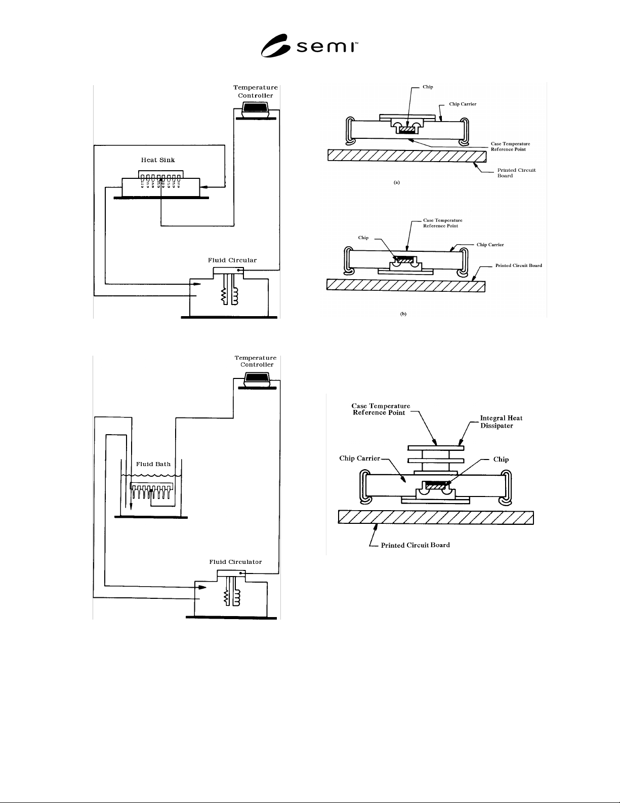
SEMI G30-88 © SEMI 1986, 19885
Figure 1
Temperature-Controlled Heat Sink Assembly
Figure 2
Temperature-Controlled Fluid Bath Assembly
Figure 3
Reference Point Location for Case Temperture
Measurement of A) Cavity-Up and B) Cavity—
Down Ceramic Packages
Figure 4
Reference Point Location for Case Temperature
Measurement of a Ceramic Package with an
Integral Head Dissipater