semi合集-English.pdf - 第7234页
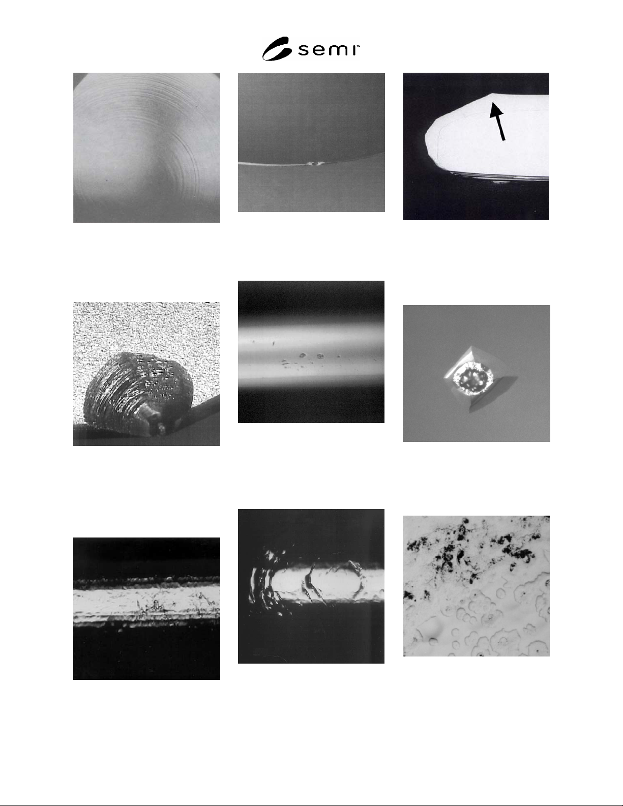
SEMI MF154-0305 © SEMI 2003, 2005 8 Figure 43 Dopant Striation Rings after Preferentially Etching, Full Wafer View Figure 44 Relatively Large Chip Found at the End of a Major Flat, No Preparation Required, Magnificati on…
SEMI MF154-0305 © SEMI 2003, 2005 7
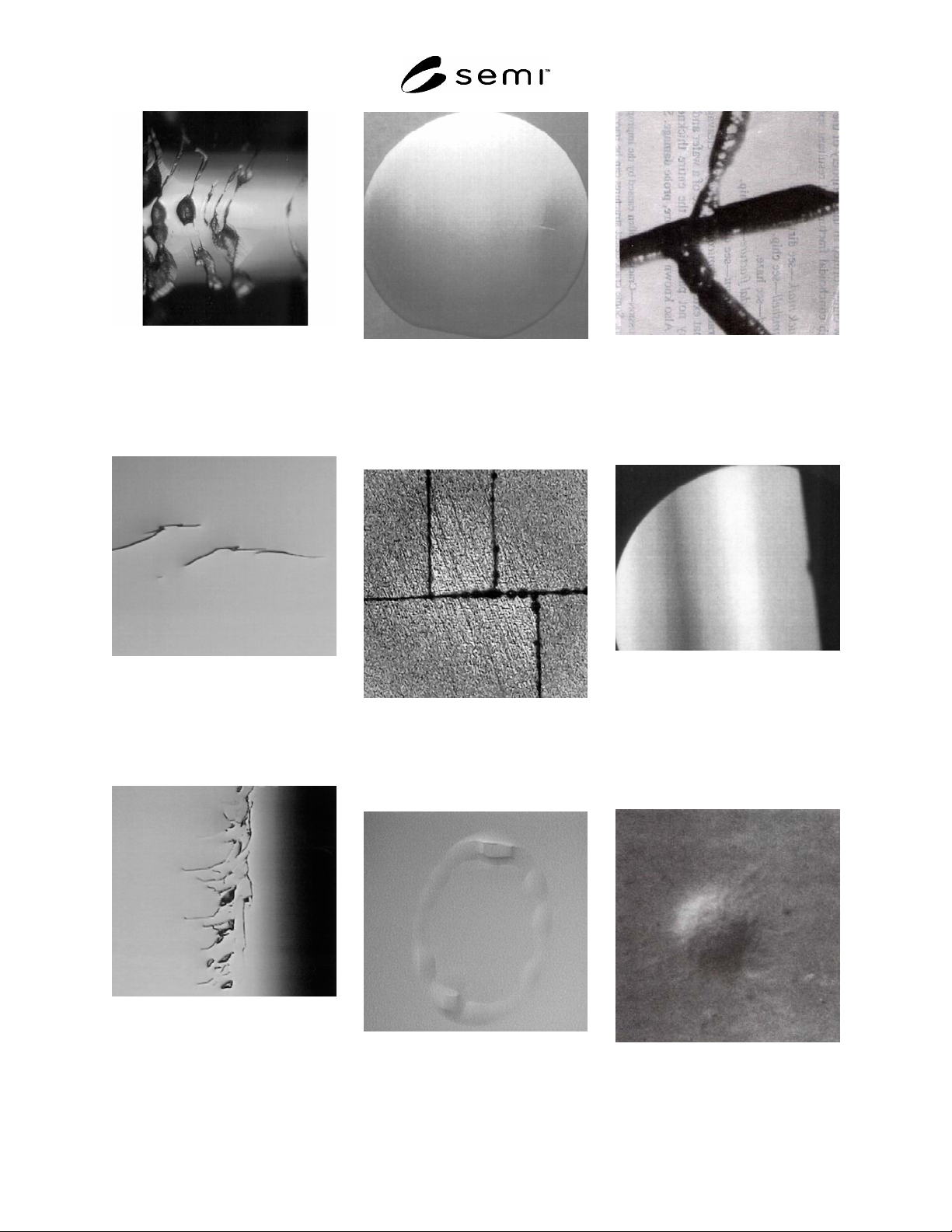
Figure 34
Crack on the Wafer Edge Due to
Mechanical Contact, No
Preparation Required,
Magnification 100×
Figure 35
Crack on a Wafer Surface Due to
Mechanical Contact, No
Preparation Required,
Magnification 750×
Figure 36
Crack Near the Edge of a Wafer
Surface Due to Mechanical
Contact, No Preparation
Required, Magnification 750×
Figure 37
Cracks in a Wafer Surface
Viewed with High Intensity Light
Exhibiting a Scratch-Like
Appearance
Figure 38
Cracks in an Etched Wafer
Surface, Magnification 38×
Figure 39
Crater, Usually Caused by
Inadequate Rinse of Polishing
Chemicals, Magnification 50×
Figure 40
“Crows-Foot” Crack Resulting
from the Impact of a Hard
Object with the Wafer
Highlighted by Preferential Etch,
Magnification 300×
Figure 41
Dimples Under Fluorescent
Lighting Conditions Distort the
Reflected Image
Figure 42
Dimple, No Preparation
Required, Magnification 512×
SEMI MF154-0305 © SEMI 2003, 2005 8
Figure 43
Dopant Striation Rings after
Preferentially Etching, Full
Wafer View
Figure 44
Relatively Large Chip Found at
the End of a Major Flat, No
Preparation Required,
Magnification 37×
Figure 45
Relatively Small Chips Found on
an Edge Face, No Preparation
Required, Magnification 100×
Figure 46
Edge Chips, Full Wafer View
Figure 47
Relatively Small Edge Chips on a
Polished Edge Face,
Magnification 200×
Figure 48
Edge Cracks on an Edge Face,
No Preparation Required,
Magnification 200×
Figure 49
Vertical Cross Section of Edge
Crown on a Cleaved Epitaxial
Wafer, Viewed With Low
Magnification, Bright Field
Microscope
Figure 50
Epitaxial Large Point Defect, No
Preparation Required,
Magnification 200×
Figure 51
Foreign Matter,
Magnification 200×
SEMI MF154-0305 © SEMI 2003, 2005 9
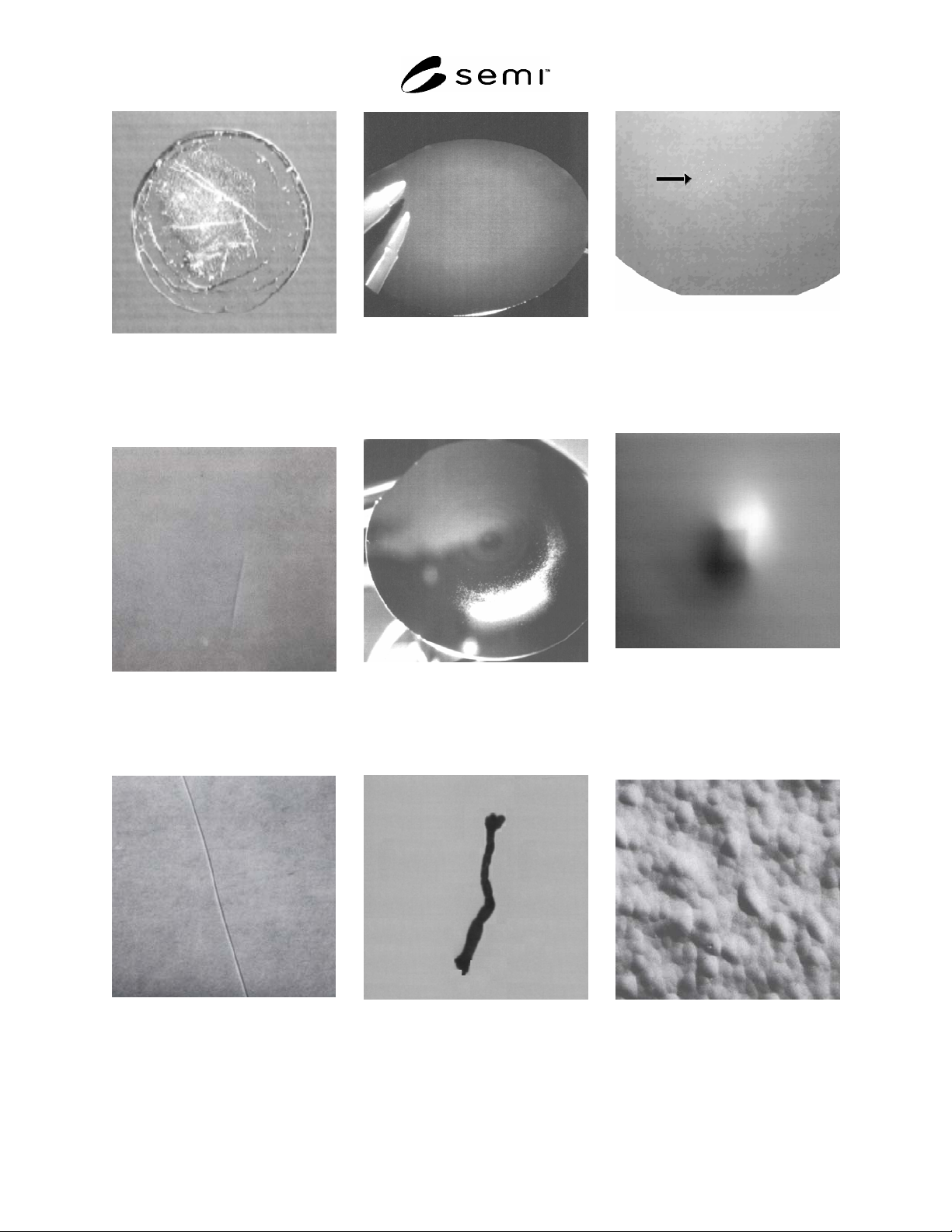
Figure 52
Foreign Matter from a Dried
Liquid Spot, Magnification 200×
Figure 53
Groove or Micro-Scratch,
Magnification 220×
Figure 54
Groove or Micro-Scratch,
Magnification 220×
Figure 55
Haze Seen as Distortion or
Blurring of a Reflected Image,
Full Wafer View
Figure 56
Haze (Extreme Case) Seen as a
White Cloudiness Under High
Intensity Light, Full Wafer View
Figure 57
Localized Light Scatterers,
(Particle Contamination) in the
Form of Small Fiber,
Magnification 200×
Figure 58
Localized Light Scatterers Seen
in High Intensity Light, Full
Wafer View
Figure 59
Mound, No Preparation
Required, Magnification 200×
Figure 60
Orange Peel Surface Roughness,
Magnification 200×