semi合集-English.pdf - 第429页
SEMI E57-0305 © SEMI 1996, 2005 5 Figure 3 Kinematic Coupling Pin Locations y 92 = 120 ± 0.05 y 93 = 64 ± 0.05 y 94 = 96 ± 0.05 y 91 = 80 ± 0.05 primary pin facial datum plane x 91 = 115 ± 0.05 x 92 =92 ± 0.05 300-mm waf…
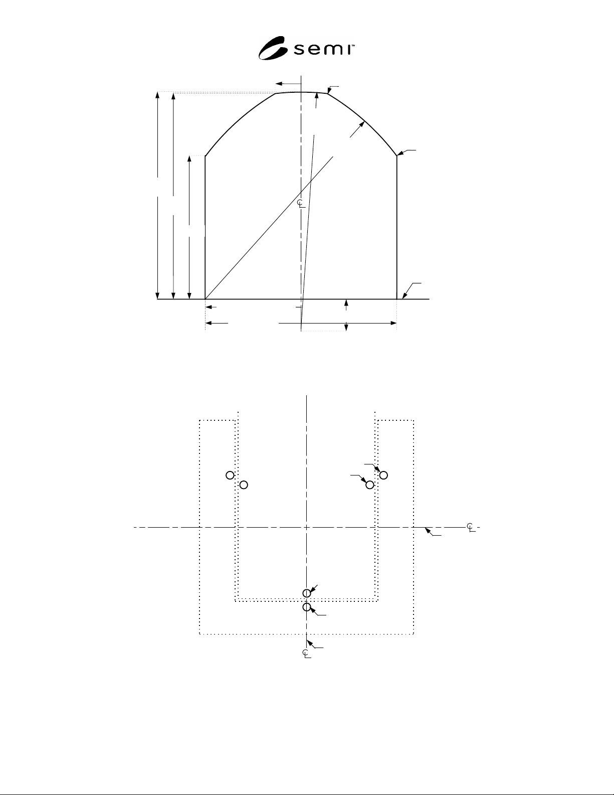
SEMI E57-0305 © SEMI 1996, 2005 4
horizontal
datum plane
r94 = 2 ± 0.1
(blend)
final roughness
height of over-all
surface finish
r9
7
0.30
m (R
a
)
(
z
93
12.910)
(
z
94
13)
(
z
92
9)
d
91 = 12 ± 0.05
r92 = 6 ± 0 (origin of r95)
(
r
91
1.637)
r96 = 2 ± 0.1
(blend)
r95
= 15 ± 0.05
r93
= 15
± 0.05
z91= 2 ± 0
Figure 1
Kinematic Coupling Pin Shape
tool
load-port
robotic
arm
primary pin
facial
datum
plane
bilateral datum plane
secondary pin
primary pin
secondary
pin
Figure 2
Primary and Secondary Kinematic Coupling Pins
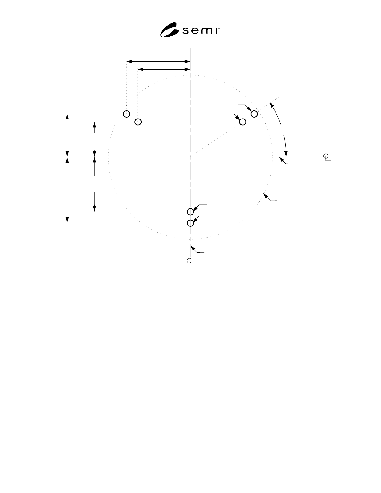
SEMI E57-0305 © SEMI 1996, 2005 5
Figure 3
Kinematic Coupling Pin Locations
y 92
= 120 ± 0.05
y
93
= 64 ± 0.05
y 94
= 96 ± 0.05
y 91
= 80 ± 0.05
primary pin
facial
datum
plane
x
91 = 115 ± 0.05
x92
=92 ± 0.05
300-mm
wafer
bilateral datum plane
34.8°)
secondary pin
primary pin
secondary
pin
SEMI E57-0305 © SEMI 1996, 2005 6
RELATED INFORMATION 1
APPLICATION NOTES
NOTICE: This related information is not an official part of SEMI E57. This related information was approved for
publication by full letter ballot procedures.
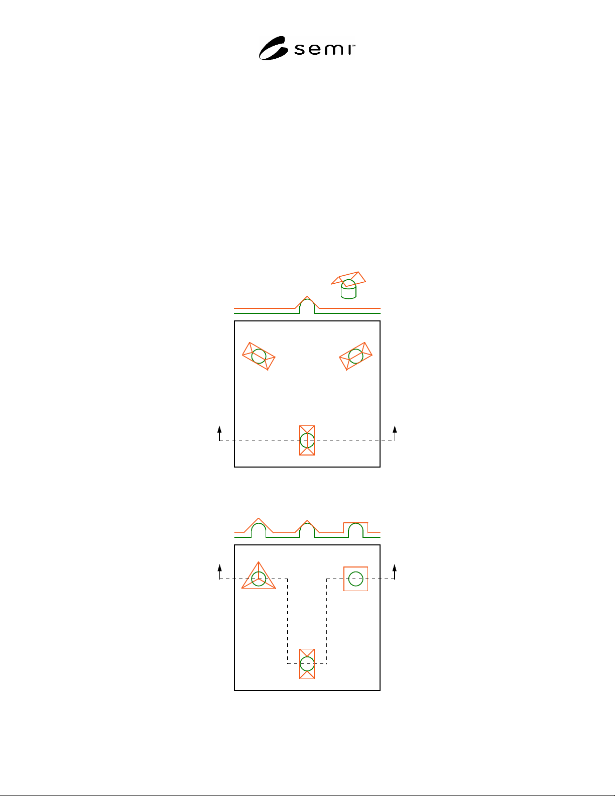
R1-1 The three features on the bottom of the wafer carrier that mate with the six pins underneath are not specified
in this standard. These three features are recommended to be inverted V-shaped grooves, each of which extends
along a line that is perpendicular to, and co-planar with, the nominal wafer center line (as shown in Figure R1-1).
Such grooves are likely to work well even when shrunken or slightly misaligned (such as when they do not all line
up with the nominal wafer center line). Other mating features are also possible, such as those shown in Figure R1-2
where one pin is contacted on the top. Front-opening boxes may need to contact the pins on the side to provide
pressure against a front mechanical interface. Such options are why the top and sides of the pins are toleranced so
tightly. When designing the mating features on the bottom of the wafer carrier, it is suggested that designers follow
the recommendations given in the book (listed in §6) by Dr. Alexander H. Slocum.
Figure R1-1
Recommended Mating Features
Figure R1-2
Alternative Mating Features