semi合集-English.pdf - 第7216页
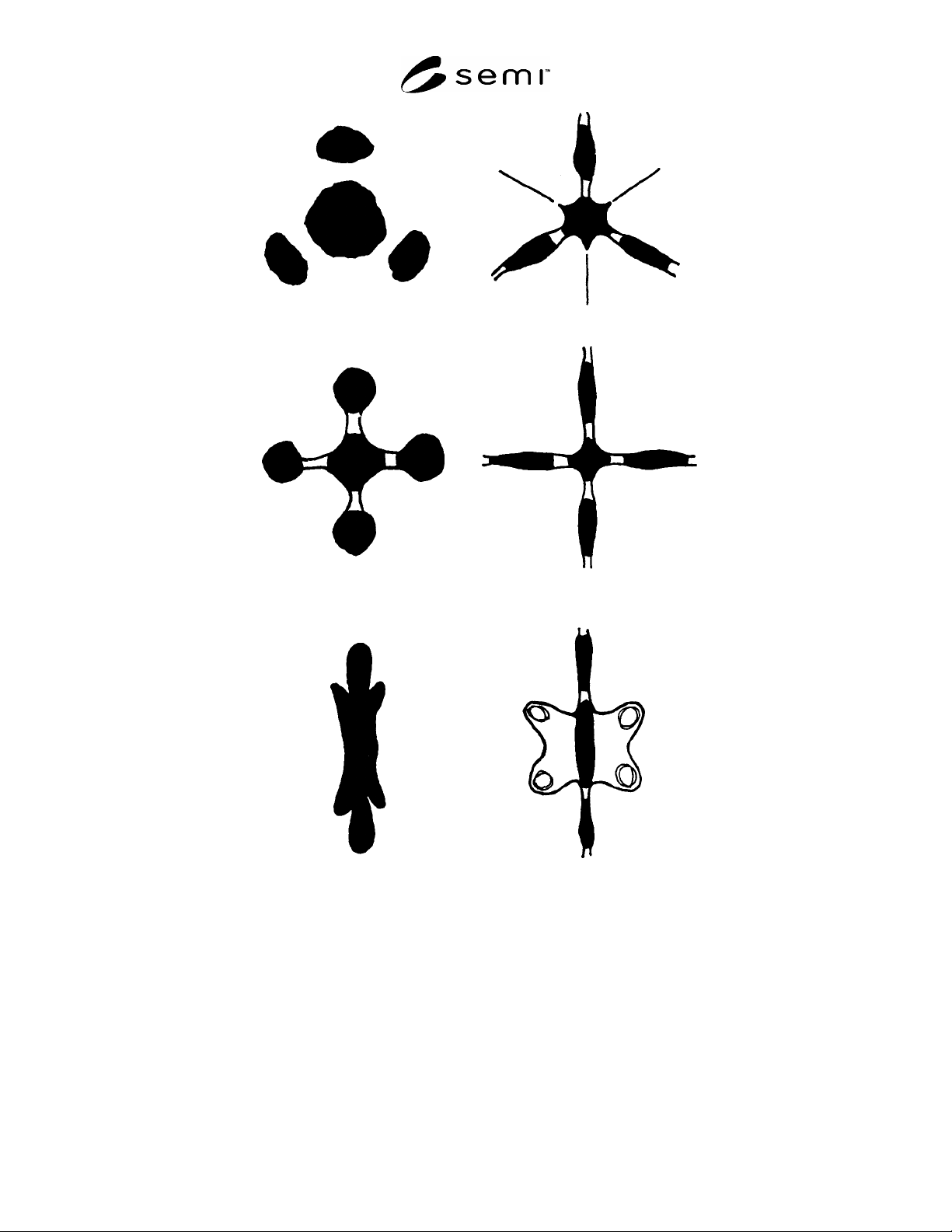
SEMI MF26-0305 © SEMI 2003, 2005 6 ( 111 ) GE RM AN IU M (110) GERMA NIUM (100) GERMA NIUM (100) SI LICON (110) SI LICON (111) SI LICON Figure 2 Optical Reflections from Etched Germanium and Silicon Surfaces 5.3.2 St age…

SEMI MF26-0305 © SEMI 2003, 2005 5
4.5.3 Calculate the instrument errors,
and
, as follows:
2
)(
31
(8)
and
2
)(
42
(9)
where
is taken from Table 1 for the crystallographic plane and material under consideration.
NOTE 2: The instrument errors need not be recorded; however, if they remain small and constant, they can be used to correct
1
and
2
so that
and
can be determined from only two measurements when the highest precision is not required. Since the
instrument error is a constant,
and
should be the same. Any difference between
and
is due to inaccuracies in one's
ability to measure
1
,
2
,
3
, and
4
. With precise measurements, the difference between
and
should be less than ½ min.
5 Test Method B — Optical Orientation
5.1 Summary of Test Method
5.1.1 When a single crystal surface of germanium or silicon is lapped and preferentially etched, numbers of
microscopic pits appear on the crystal surface. These pits are bounded by planes related to the principal
crystallographic directions of the material. These limiting boundary planes determine the shape of the pits when the
etched surface is near a major crystallographic direction. An optical examination of the facets comprising the pit
walls relates the crystal surface under examination to this crystallographic direction, and further permits a
determination of the degree of misorientation of the surface from the crystallographic plane.
5.1.2
A light beam that is reflected from such a preferentially etched surface may be focused upon a screen to form
a definite geometric pattern characteristic of the surface etch pit structure. Patterns, such as those reproduced in
Figure 2, reflected from surfaces approximately parallel to (111)-, (100)-, and (110)-type planes are recognizable. In
each instance, the central portion of the pattern observed on the screen is the reflection from the bottom of the etch
pit. These bottom facets represent planes parallel to the characteristic crystallographic plane of the surface under
investigation. Therefore, when the central reflected beam is aligned with the direction of the light beam, this
crystallographic plane is perpendicular to the light beam direction. This observation permits orientation of the
crystal along a desired crystallographic axis or, alternatively, allows the determination of the degree of
misorientation of a crystal surface from a desired crystallographic plane.
5.2
Reagents and Materials
5.2.1 Purity of Water — Reference to water shall be understood to mean Type E-3 or better water as described in
ASTM Guide D 5127.
5.2.2
Germanium Etchant Solution — Mix 1 part HF, 1 part H
2
O
2
, and 4 parts water, by volume.
5.2.3 Hydrofluoric Acid (HF), 49%, in accordance with Grade 1 of SEMI C28.
5.2.4 Hydrogen Peroxide (H
2
O
2
), 30%, in accordance with Grade 1 of SEMI C30.
5.2.5 Potassium Hydroxide Solution (KOH), 45% by weight in water, in accordance with Grade 1 of SEMI C40.
5.2.6 Sodium Hydroxide Solution (NaOH), 50% by weight in water, in accordance with Grade 1 of SEMI C43.
5.3 Apparatus
5.3.1 Light Beam — originating preferably from a high-intensity point source. An image of the source shall be
observed on a screen following reflection from a front surface mirror occupying the crystal test position. This image
establishes the zero reference point. The angle of incidence at the reflecting surface may be 0° of arc, in which case
a hole must be provided at the center of the screen to permit passage of the incident light beam. The angle of
incidence may be made large enough to permit the screen to be displaced to one side of the light beam. In this
arrangement, it is essential that the screen be placed in the focal plane of the lens system to minimize distortion of
the image.
SEMI MF26-0305 © SEMI 2003, 2005 6
(
111
)
GERMANIUM
(110) GERMANIUM
(100) GERMANIUM
(100) SILICON
(110) SILICON
(111) SILICON
Figure 2
Optical Reflections from Etched Germanium and Silicon Surfaces
5.3.2 Stage — capable of rotation both vertically and horizontally and calibrated to permit measurements of
deviation from the 0° reference plane. Means shall be provided to securely position the reflecting surface of the
crystal on the stage of the apparatus.
5.4 Procedure
5.4.1 Abrade the specimen surface by lapping with No. 600 silicon carbide abrasive. The abrasive grain size
specified for this purpose shall comply with the appropriate specifications of ANSI B74.10. Care must be taken to
produce no angular deviation from the original surface during the lapping operation.

SEMI MF26-0305 © SEMI 2003, 2005 7
5.4.2 Etch the lapped surface as follows:
5.4.2.1 Etch germanium surfaces with germanium etchant solution (see ¶5.2.2) for 1 min at 25C.
5.4.2.2 Etch silicon surfaces with 45% KOH solution (see ¶5.2.5) or 50% NaOH solution (see ¶5.2.6) for 5 min at
65C.
5.4.3 Mount the specimen containing the prepared surface on the goniometer in the path of the incident light beam.
5.4.4 Adjust the position of the specimen surface to bring the center of the reflected light pattern to the zero
reference point described in ¶5.3.1. The angular reading on the goniometer required to make this adjustment is the
degree of misorientation on the surface under examination.
5.4.5
Check this measurement, where possible, by rotating the surface through 180° of arc. The angular deviation
must remain constant in magnitude but is opposite in sign.
5.4.6 Rotate the specimen through 90° of arc about a normal to the surface under investigation, and repeat the
procedure to measure the second component of angular deviation.
5.5 Calculations
5.5.1 Calculate and record the total angular deviation,
, in accordance with ¶4.5.2.
6 Report
6.1 Report the following information:
6.1.1 Method used (X-ray or optical),
6.1.2 Material investigated,
6.1.3 Crystal reference plane,
6.1.4 Deviation of prepared surface from this reference plane in two mutually perpendicular directions, and
6.1.5 Total angular deviation of prepared surface from the reference plane
7 Precision and Bias
7.1 Test Method A, X-ray Diffraction Orientation — The single instrument precision of the method as defined in
ASTM Practice E 177 is ±15 min of arc (3S) using commercially available X-ray equipment.
7.2 Test Method B, Optical Orientation — The single instrument precision of the method as defined in ASTM
Practice E 177 is ±30 min of arc (3S) using commercially available optical orientation equipment.
8 Keywords
germanium; orientation; preferential etch; semiconductor; silicon; X-ray diffraction
NOTICE: SEMI makes no warranties or representations as to the suitability of the standards set forth herein for any
particular application. The determination of the suitability of the standard is solely the responsibility of the user.
Users are cautioned to refer to manufacturer's instructions, product labels, product data sheets, and other relevant
literature, respecting any materials or equipment mentioned herein. These standards are subject to change without
notice.
By publication of this standard, Semiconductor Equipment and Materials International (SEMI) takes no position
respecting the validity of any patent rights or copyrights asserted in connection with any items mentioned in this
standard. Users of this standard are expressly advised that determination of any such patent rights or copyrights, and
the risk of infringement of such rights are entirely their own responsibility.
Copyright by SEMI® (Semiconductor Equipment and Materials
International), 3081 Zanker Road, San Jose, CA 95134. Reproduction of
the contents in whole or in part is forbidden without express written
consent of SEMI.