semi合集-English.pdf - 第6031页
SEMI G3-90 © SEMI 1 980, 199 6 3 6 Mat erials 6.1 Ceramic 6.1.1 A lumina content 90% minimu m . 6.1.2 Color — Opaque or white. 6.2 Metallization 6.2.1 Refractor y m etallization (prov i d e adequate bo nd strength to cer…
SEMI G3-90 © SEMI 1980, 1996 2
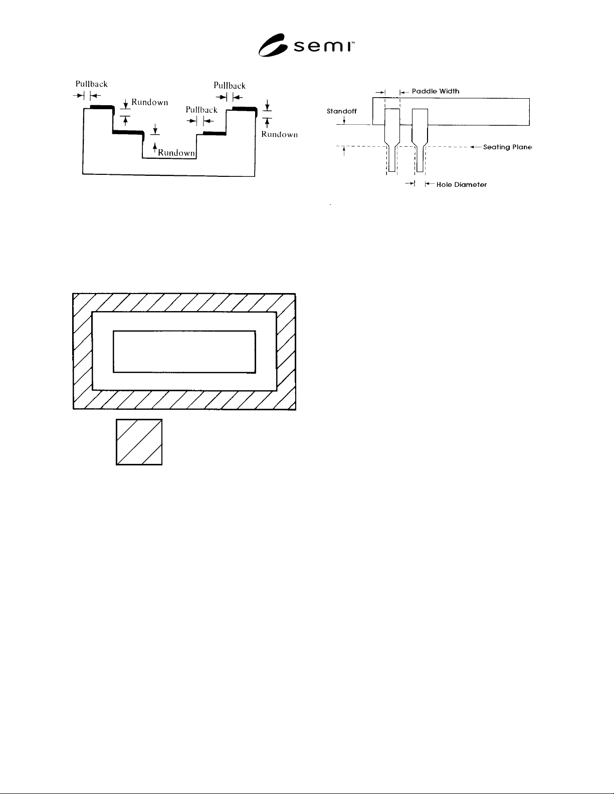
Figure 3
Metallization Misalignment
SSI — Small scale integration.
seal area — A dimensional outline area designated for
either metallization or bare ceramic to provide a surface
area for sealing. (See Figure 4.)
Figure 4
Seal Area
seating plane — See Figure 5.
standoff — Residual air gap after inserting the leads
into a ground steel plate with a specific size hole and
applying a specified downward pressure. (See Figure
5.)
NOTE: When determining the seating plane a downward
f
of 10 grams is to be applied to the package.
Figure 5
Leadframe Paddle Width and Standoff
TIR — Total indicator reading.
VLSI — Very large scale integration.
void — An absence of metallization or plating from a
designated area.
4 Ordering Information
Purchase orders for sidebrazed laminated packages
furnished to this specification shall include the
following items:
1. Drawing number and revision level
2. Number of leads and lead series spacing
3. Type and color of ceramic
4. Type and thickness of plating
5. Description (See Table 1.)
6. Thickness of individual layers of ceramic
7. Internal finger bonding pattern layout
8. Minimum exposed metallized bond finger length
and width
9. Leads common to die attach area and/or seal ring
10. Sealing dimensions and flatness
11. Certification
12. Method of test and measurements (See Section 9.)
13. Lot acceptance procedures (See Section 8.)
14. Packaging and Marking (See Section 10.)
5 Dimensions and Permissi ble Variations
The dimensions of the sidebraze laminate packages
shall conform as specified in Table 1.

SEMI G3-90 © SEMI 1980, 19963
6 Materials
6.1 Ceramic
6.1.1 Alumina content 90% minimum.
6.1.2 Color — Opaque or white.
6.2 Metallization
6.2.1 Refractory metallization (provide adequate bond
strength to ceramic).
6.2.2 Nickel plating (if designated).
6.2.3 Precious or noble metal plating.
6.2.4 Nickel/gold per MIL-M-38510 except gold
plating shall conform to MIL-G-45204, Type III and
have a thickness of 60 microinches minimum.
6.3 Braze Material — An alloy with a melting point
equal to or greater than 750°C which will provide
specified bond strength of the lead to the ceramic.
6.4 Lead Material
6.4.1 Iron nickel cobalt alloy per MIL-M-38510, Type
A.
6.4.2 Iron nickel alloy per MIL-M-38510, Type B.
7 Defect Limits
7.1 Ceramic
7.1.1 Cracks — None allowed.
7.1.2 Chips
7.1.2.1 Corner — 0.762 mm (0.030") × 0.762 mm
(0.030") × 0.762 mm (0.030") max.
7.1.2.2 Edge — 2.54 mm (0.100") × 0.762 mm
(0.030") × 0.762 mm (0.030") max. (Chips can not be
encroached or exposed any metallized area.)
7.1.2.3 Seal Area
7.1.2.3.1 7.62 mm (0.300") and 10.16 mm (0.400")
Row Spacing Parts — .762 mm (0.030") × 2.54 mm
(0.100")
7.1.2.3.2 15.24 mm (0.600") Row Spacing Parts —
1.27 mm (0.050") × 0.381 mm (0.015") × 0.381 mm
(0.015") max.
7.1.2.3.3 22.86 mm (0.900") Rowing Spacing Parts —
1.52 mm (0.060") × 0.508 mm (0.020") × 0.508 mm
(0.020") max.
7.1.2.3.4 Chips cannot reduce the seal width by more
than 1/3 of the design width.
7.1.3 Burrs and Projections
7.1.3.1 Top Plane Excluding Seal Area — 0.102 mm
(0.004") max.
7.1.3.2 Seal Area — 0.025 mm (0.001") max. above
metallization.
7.1.3.3 Wire Bond Finger Areas — 0.025 mm (0.001")
max. above metallization.
7.1.3.4 Die Attach Surface — 0.025 mm (0.001") max.
above metallization excluding a 0.203 mm (0.008")
perimeter on 7.62 mm (0.300") centerline packages,
0.254 mm (0.010") perimeter on 10.16 mm (0.400")
centerline packages and 0.381 mm (0.015") perimeter
on 15.24 mm (0.600") centerline packages, 0.508 mm
(0.020") perimeter on 22.86 mm (0.900") row center
package.
7.1.4 Camber — Ceramic-maximum of 0.004
inch/inch (mm/mm).
7.1.5 Flatness
7.1.5.1 Seal Area — 0.050 mm (0.002") TIR on 7.62
mm (0.300") row center packages, 0.0635 mm
(0.0025") TIR on 10.16 mm (0.400") and 15.24 mm
(0.600") row center packages.
7.1.5.2 Die Attach — Die attach pad to be flat to
within 0.051 mm (0.002") TIR to exclude a 0.203 mm
(0.008") perimeter on 7.62 mm (0.300") centerline
packages, 0.254 mm (0.010") perimeter on 10.16 mm
(0.400") centerline packages and 0.381 mm (0.015")
perimeter on 15.24 mm (0.600") centerline packages.
7.2 Metallization
7.2.1 Voids
7.2.1.1 Seal Area — On the outer half of the seal area
width, maximum of 3 voids no larger than 0.127 mm
(0.005") in diameter are permissible. On the inner half,
maximum of 3 voids no larger than 0.381 mm (0.015")
in diameter or larger than 1/3 of the seal area width,
whichever is the smaller. The distance between any 2
voids shall be at least 0.762 mm (0.030").
7.2.1.2 Wire Bond Fingers — A 0.254 mm (0.010") ×
0.010" (0.254 mm) void free area within the specified
wire bond finger area as defined be the procurement
drawing.
7.2.1.3 Die Attach Surface — Maximum 0.010"
(0.254 mm) diameter by a distance greater than 0.030"
(0.762 mm) with no more than 3 voids.
7.2.2 Metallization Misalignment — See Figure 3.
7.2.2.1 Seal Plane Rundown — Internal cavity — not
to exceed 25% of the cavity layer thickness. External
cavity — not to be less than 0.010" (0.254 mm) outside
the cavity.

SEMI G3-90 © SEMI 1980, 1996 4
7.2.2.2 Wire Bond Finger Pullback — A 0.010"
(0.254 mm) maximum from the cavity edge and the
minimum exposed wire bond lead length must meet the
dimension on the procurement drawing or specification.
7.2.2.3 Wire Bond Finger Rundown — Not to exceed
25% of the ceramic layer thickness or 0.005" (0.127
mm), whichever is the smaller.
7.3 Lead Attachment
7.3.1 Voids in Braze
7.3.1.1 Gold Plated Leadframes — 75% of the braze
fillet will be void free.
7.3.1.2 Nickel or Bare Leadframes — 75% of the
braze fillet will be void free.
7.3.2 Lead Alignment
7.3.2.1 Misalignment Leads to Braze Pads — The
leads shall not overhang the braze pads by more than
25% of the measured paddle width nor reduce the
clearance between adjacent pad or lead to less than 50%
of the clearance between adjacent metallizations.
7.3.2.2 Lead Offset — Lead centerlines must be
aligned to within 0.015" (0.381 mm) relative to the
position of the leads on the opposite side of the
package.
7.3.2.3 Lead-to-Lead Alignment — 0.010" ± 0.010"
(0.254 mm ± 0.254 mm) measured at the base of the
ceramic on the same side.
8 Sampling
Sampling sizes must meet the requirements of MIL-
STD-105; although single, double, or multiple samples
may be used.
9 Test Methods
9.1 Mechanical, Electrical and Thermal Test Methods
9.1.1 Gold Plating Quality
9.1.1.1 Purity and adhesion of the gold plated package
shall be tested by placing parts on a calibrated heater
block at:
Condition A — 450°C ± 10°C for two minutes in air, or
Condition B — 470°C ± 10°C for one minute in
nitrogen.
9.1.1.2 After cooling at room temperature the
packages will be visually examined for the following
criteria:
9.1.1.2.1 Blisters on the leadframe are acceptable only
on the tie bar (that portion removed during trim).
Blisters on the bonding fingers shall not exceed 0.003"
(0.076 mm) diameter with a maximum of 1 blister per
finger and 5 blisters per package of any size. Blisters on
the seal ring shall not exceed 0.005" (0.127 mm)
diameter. Blisters on the die attach pad shall not exceed
0.010" (0.254 mm) diameter with a maximum of 5
blisters per package greater than 0.005" (0.127 mm)
diameter.
9.1.1.2.2 Slight discoloration of the gold at the die
attach pad edges up to 0.025" (0.635 mm) from the
cavity walls is acceptable. Discoloration of the bonding
fingers, seal ring surface or external leads is not
acceptable.
9.1.1.2.3 There shall be no flaking or peeling of the
package plating when viewed at 15× magnification.
9.1.1.2.4 Superficial stains left during drying or prior
operations is not cause for rejection.
9.1.2 Lead Pull — Four pounds (1.8 kg) minimum at a
45° angle from the lead’s original plane.
9.1.3 Lead Fatigue — Test per MIL-STD-883,
Method 2004.2, Test Condition B2, Section 3.2.
9.1.4 Thermal Characteristics — Test per MIL-STD-
883, Method 1012, Test Conditions A, B, C, D, and E.
9.2 Functional Test Methods
9.2.1 Die Attach Quality — Perform destructive die
shear test post environmental testing per MIL-STD-
883, Method 2019.1, Section 3.2C.
9.2.2 Wire Bond Quality — Perform minimum pre-
seal and post-seal bond strength test per MIL-STD-883,
Method 2011.2, Test Condition D. Reject for bonds
which cause plating to lift from the base metal of the
die attach surface or bonding fingers.
9.2.3 Solderability — Test per MIL-STD-883, Method
2003.2.
9.2.4 Insulation Resistance — Test per MIL-STD-883,
Method 1003.
9.2.5 Hermetic and Environmental Testing
9.2.5.1 The hermetic integrity of the package must be
maintained after all environmental testing. Hermetic
checks shall comply with MIL-STD-883, Method
1014.3, Test Condition A
1
or B and C.
9.2.5.2 Environmental testing shall include, but not be
limited to, the following:
1. Temperature Cycle — MIL-STD-883, Method
1010.2 Condition C
2. Thermal Shock — MIL-STD-883, Method 1011.2,
Condition C