semi合集-English.pdf - 第4454页
SEMI D13-1101 © SEMI 1995, 2001 2 may vary to suit the application. T hese are illustrated in Figure 2. 7 Color Filter Types and Fab r i ca tion Methods 7.1 Fabr ication Metho ds 7.1.1 photolith ography — Patterning me t…
1 SEMI D13-1101 © SEMI 1995, 2001
SEMI D13-1101
TERMINOLOGY FOR FPD COLOR FILTER ASSEMBLIES
These specifications were technically approved by the Committee and are the direct responsibility of the
Japanese FPD Materials and Components Committee. Current edition approved by the Japanese Regional
Standards Committee on April 19, 2001. Initially available at www.semi.org August 2001; to be published
November 2001. This document was originally published in 1995.
1 Purpose
1.1 These terms and definitions describe various
elements and characteristics of FPD color filter (CF)
assemblies. They are intended to assist in future CF
standardization activity.
2 Scope
2.1 Color filters comprise the front plate assembly in a
colored flat panel display. They consist of a number of
material layers such as glass substrate, color filter layer,
black matrix, overcoat layer, and Indium Tin Oxide
(ITO) films. Each of these layers has various properties
which may need to be specified, produced, controlled,
and characterized. This document provides an overview
of these layers, with terms and definitions for selected
elements, and indicates the appearance of some color
filter defects. This document may be useful in
developing material specifications, inspection criteria,
and test methods.
2.2 This standard does not purport to address safety
issues, if any, associated with its use. It is the
responsibility of the user of this standard to establish
appropriate safety and health practices and determine
the applicability of regulatory limitations prior to use.
3 Limitations
3.1 This document does not contain detailed
measuring and test methods. Such methods may be
developed separately, and references to them may be
incorporated into color filter specification documents
where appropriate. The assembly of color filters into a
flat panel display assembly is not covered herein.
4 Related Standards
4.1 SEMI Standards
SEMI D3 — Quality Area Specification for Flat Panel
Display Substrates
SEMI D20 Defect Terminology for Flat Panel
Display Masks
SEMI D21 Terminology for Flat Panel Display
Masks
SEMI M21 — Specification for Assigning Addresses to
Rectangular Elements in a Cartesian Array
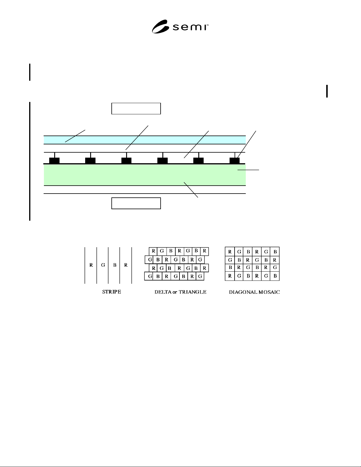
5 Color Filter Elements (see Figure 1)
5.1 alignment control projection
a rib-shaped
protrusion created within the display pixel on the color
filter film surface for the purpose of controlling
alignment direction of the liquid crystal.
5.2 backside ITO film
a thin film of Indium Tin
Oxide formed on the glass surface on the back of the
color filter substrate.
5.3 black matrix (BM) — layer which blocks light
transmission. It provides a boundary between color
filter pixels, preventing the transmitting light between
adjacent pixels.
5.4 color filter layer — colored layer through which
light is transmitted. It is deposited in three colors—red,
green, and blue—which are patterned to produce an
array of contiguous, rectangular, or square-shaped
pixels.
5.5 glass substrate — the base material onto which
black matrix and color filter layer are deposited. Also
called the Front Plate. After assembly into a Display, its
back surface faces the observer. See SEMI D3 and
SEMI D21 for parameters, definitions, and dimensional
specifications.
5.6 ITO Film — a thin film of Indium Tin Oxide.
5.7 overcoat layer — transparent material deposited
over the color filter material. This provides a smooth
surface and enough adhesion for subsequent ITO
material deposition.
5.8 post spacer
a fixed pillar-shaped spacer formed
outside of the pixel opening.
5.9 reflective film
a light-reflective layer created on
the color filter substrate below the color filter layer.
6 Color Filter Pixel (RGB) La yout
6.1 The color filter pixels are arranged in one of
several array patterns. The array is constructed from m
vertical columns and n horizontal rows of identical
pixels of dimensions a horizontally and b vertically.
The number of pixels in different rows and columns
SEMI D13-1101 © SEMI 1995, 2001 2
may vary to suit the application. These are illustrated in
Figure 2.
7 Color Filter Types and Fabrication Methods
7.1 Fabrication Methods
7.1.1 photolithography — Patterning method by using
micro photolithograph machines and photopatternable
materials. Precise patterns can be formed.
7.1.2 color photoresist method
Defined as color
photoresist, it is possible to create a pattern through a
direct exposure method using color pigment or dye
dispersed on a photoresist.
7.1.3 dyeing — Dyeable photoresist materials are
patterned by photolithographic image processing.
These patterned materials are dyed by a special method.
The various colors may be introduced sequentially.
7.1.4 etching — Dye or pigment-dispersed color
material is coated on substrate, and it is patterned by
photolithographic etching method.
7.1.5 printing — Pigment-dispersed color ink is placed
and patterned on the substrate by printing method.
7.1.6 electric deposition — Micro cells capsulating
pigment particles are dispersed in water solvent and
deposited on the selected electrode on glass substrate.
7.1.6.1 patterned ITO method
Color filter layers are
accumulated using a micell distribution liquid for each
color of the ITO pattern formed according to the
various RGB color filter layers.
7.1.6.2 resist pattern method
Color filter layers are
accumulated on non-patterned ITO film by using a
micell distribution liquid through openings (windows)
in the photoresist according to the RGB pattern.
7.1.7 multi-layer interference CF (Dichroic CF) —
Multiple layers of inorganic transparent thin films are
patterned by photolithography method.
7.1.8 ink jet method
Color filter layers are formed
by pigment or dye-colored ink blown out from an ink
jet head nozzle onto the substrate pixels.
7.1.9 others
Fabrication methods other than those
above.
7.2 coloring materials
Other than the multi-layer
interference method, these are formed using pigments
or dyes.
7.2.1 pigment
This can be pigment in fine powder
form dispersed into plastic, or it can be pigment in fine
powder form then capsulated in micell (microcell) and
dispersed in a water solution.
7.2.2 dye
Patterned plastic or gelatin is colored
using dye. Also, dyed plastic or gelatin can be patterned
using photolithography.
7.2.3 inorganic permeable thin film
A clear thin
film of inorganic material formed through methods
such as vacuum deposition or sputtering.
7.2.4 Other
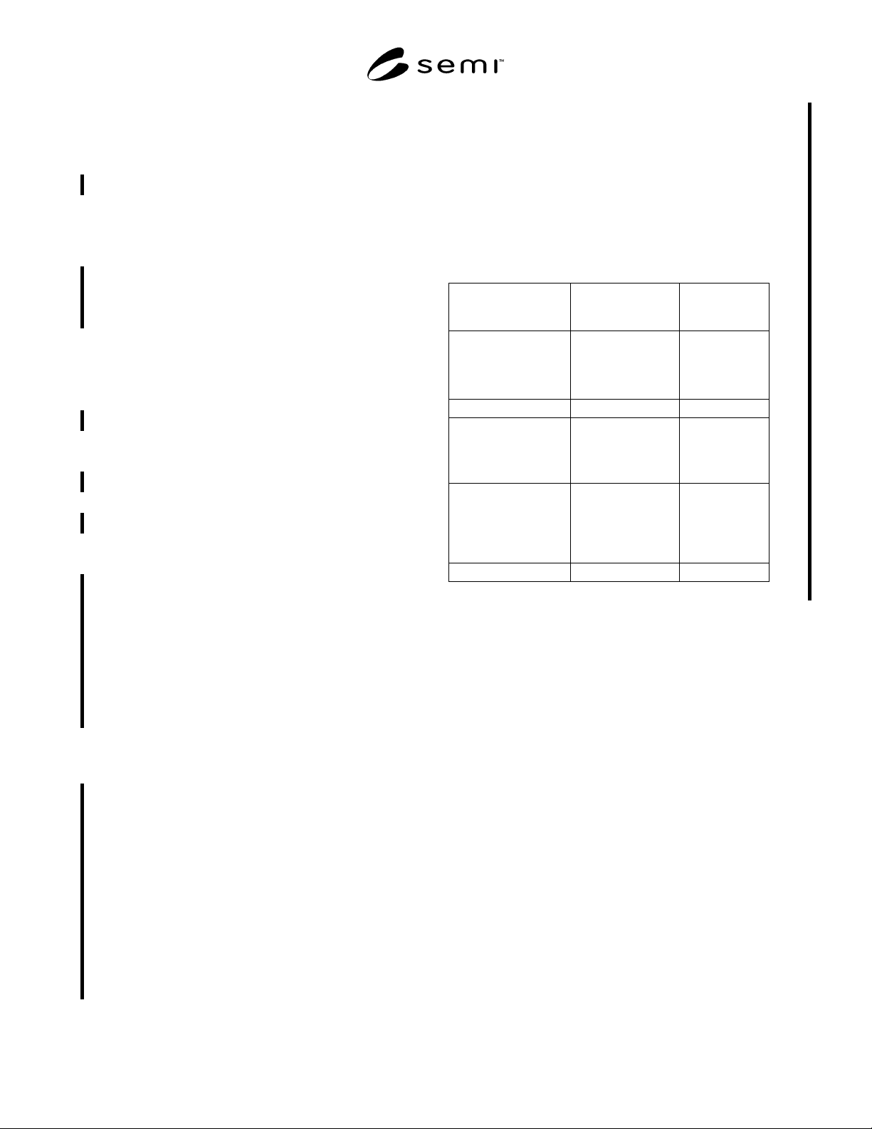
Table 1 Color Filter Fabrication Methods and
Materials
Fabrication Method
(main category)
Fabrication
Method
(subcategory)
Material
Photolithography Color Resist
Method
Dyeing Method
Etching Method
Pigment/Dye
Dye
Pigment/Dye
Printing Pigment
Electric Disposition Patterned-ITO
Method
Resist Pattern
Method
Pigment
Pigment
Mulit-layer
Interference
Vacuum
Evaporation
Method
Sputtering
Method
Inorganic
Material
Inorganic
Materials
Ink Jet Method Pigment/Dye
8 Visible Defects
8.1 black defect — Black dot-shaped defect existing in
the quality area that can be detected using transmitted
light.
8.2 white defect — White dot-shaped defect existing
in the quality area that can be detected using
transmitted light.
8.3 BM (Black Matrix) spot — A dot-shaped defect
caused by extraneous BM material deposited within the
quality area, not related to the BM pattern.
8.4 BM (Black Matrix) pin hole or pinhole — A dot-
shaped defect located within the BM pattern.
8.5 decolorant — The absence of a color element in a
normally tri-colored pixel. This may occur in a partial
area of one pixel.
8.6 color non-uniformity — Variation in brightness or
chromaticity within the quality area.
8.7 color spot — A mixing or overlapping of color
materials within an RGB pixel.
3 SEMI D13-1101 © SEMI 1995, 2001
8.8 reflectance non-uniformity — Variation in
reflectance of the surface of color filter within the
quality area.
8.9 hill — A gently sloping projection smaller than the
cell gap width. Will cause cell gap defect.
8.10 stain — A small-area spot, with no appreciable
thickness, on the surface of some color filter material.
It may be caused by introduction of foreign substances
during processing.
8.11 layer particle — A three-dimensional substance
adhered to the surface of some color filter layer
material.
8.12 protrusion
A large, severe projection larger
than the cell gap width. Will cause cell gap defect.
‚ q ‚ f ‚ a ‚ q ‚ f
ITO Film
Overcoat Layer
Color Filter Layer
Film Side
Back Side ITO Film
Back Side
Black Matrix
Glass Substrate
Figure 1
Color Filter Elements
Figure 2
Color Filter Array Patterns
NOTICE: SEMI makes no warranties or representations as to the suitability of the standards set forth herein for any
particular application. The determination of the suitability of the standard is solely the responsibility of the user.
Users are cautioned to refer to manufacturer’s instructions, product labels, product data sheets, and other relevant
literature respecting any materials mentioned herein. These standards are subject to change without notice.
The user’s attention is called to the possibility that compliance with this standard may require use of copyrighted
material or of an invention covered by patent rights. By publication of this standard, SEMI takes no position
respecting the validity of any patent rights or copyrights asserted in connection with any item mentioned in this
standard. Users of this standard are expressly advised that determination of any such patent rights or copyrights, and
the risk of infringement of such rights, are entirely their own responsibility.
Copyright by SEMI® (Semiconductor Equipment and Materials
International), 3081 Zanker Road, San Jose, CA 95134. Reproduction o
f
the contents in whole or in part is forbidden without express written
consent of SEMI.