semi合集-English.pdf - 第5384页
SEMI M55.2-0705 © SEMI 2005 3 Table 3 Polished Wafer Defect Limits Item Characteristics Maximum De fect Limit Test Condition Note Front Surface 1 visible scratches None hi gh intensity, unaided eye 1 2 pits (number) 10 h…
SEMI M55.2-0705 © SEMI 2005 2
Property Dimension
SURFACE ORIENTATION
#1, #2
Tilt angle (see Figure 2 in SEMI M55)
Option 2: “off axis (11
20)”
4.0° 0.5° parallel to edge of primary flat away from secondary flat
#3
Option 3: “off axis (11
20)”
8.0° 0.5° parallel to edge of primary flat away from secondary flat
#3
Option 4: “off axis (1
100)”
4.0° 0.5° parallel to edge of secondary flat away from primary flat
#3
Option 5: “off axis (1
100)”
8.0° 0.5° parallel to edge of secondary flat away from primary flat
#3
ORTHOGONAL MISORIENTATION
5° (See Figure 2 in SEMI M55)
TOLERANCE OF PRIMARY FLAT
ORIENTATION
2°
TOLERANCE OF SECONDARY FLAT
ORIENTATION
#2
5° relative to primary flat
#1
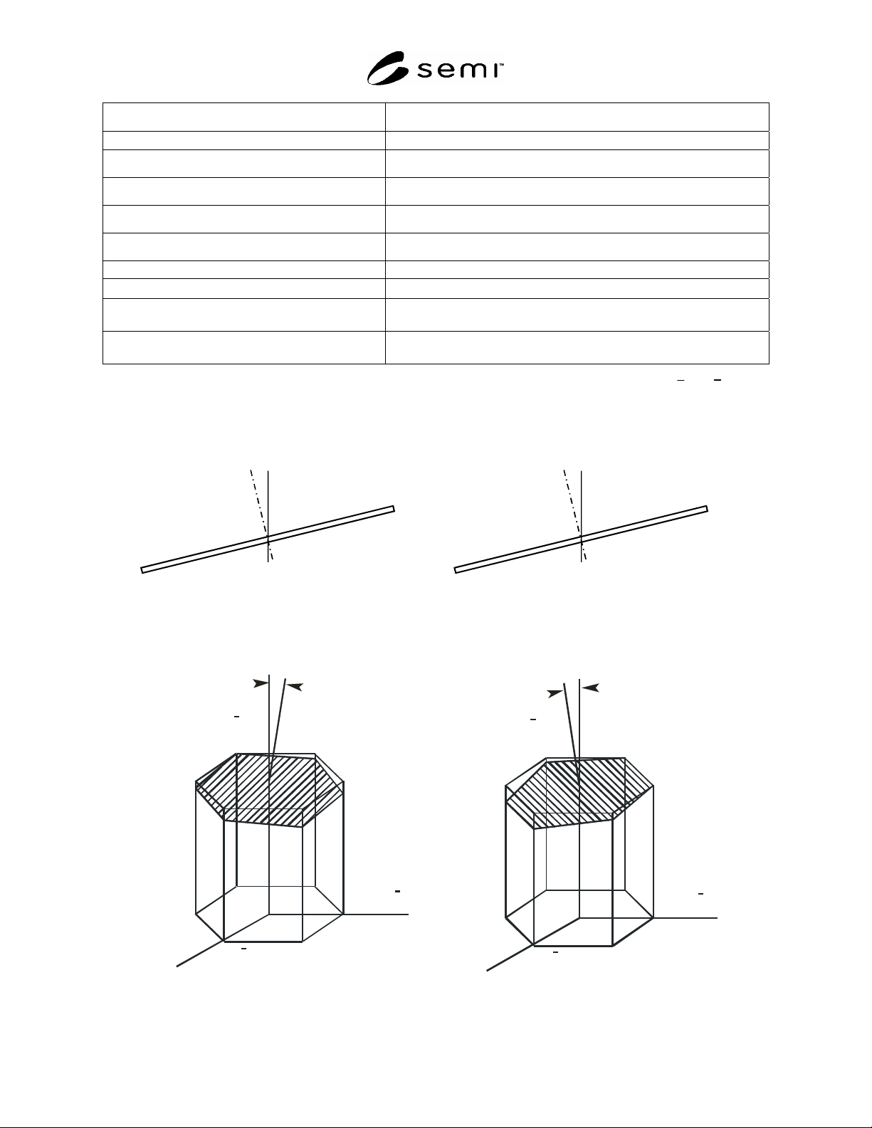
The frame of reference is the (0001)-plane of the crystal. It is the wafer normal on the silicon-face that is tilted towards the given
crystallographic direction. That means that the crystallographic c-axis lies between the secondary/primary flat (for the (1120) / (1100) option
respectively) and the silicon-face surface normal vector (See Figure 1 and 2).
#2
Measured at the center of the wafer.
#3
The angle between primary and secondary flat is defined in Figure 5 in SEMI M55.
Secondary flat
Si-face
Normal vector to
wafer surface
Crystallographic
c-axis
C-face
Primary flat
Si-face
Normal vector to
wafer surface
Crystallographic
c-axis
C-face
Figure 1
Definition of the Direction of the Tilt Angle (Left: Off Axis (11
-
20) -Option, Right Off Axis (1
-
100) Option)
tilt angle tilt angle
off towards [1120]
direction
off towards [1100]
dir ec ti o n
[1120]
direction
[1120]
direction
(1100) plane
(1100) p lan e
Figure 2
Direction of tilt (left: (11
-
20) option, right off axis (1
-
100) -option)
SEMI M55.2-0705 © SEMI 2005 3
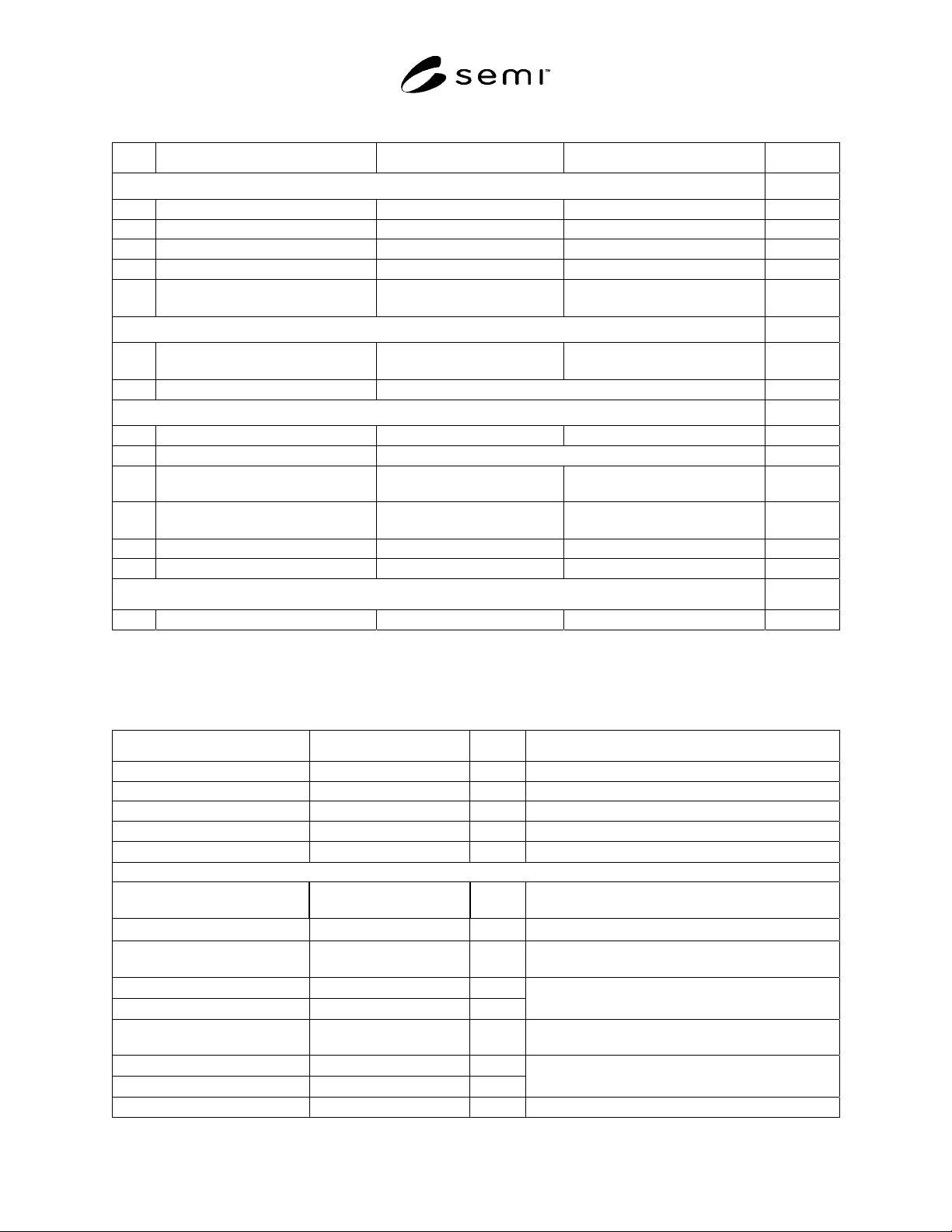
Table 3 Polished Wafer Defect Limits
Item Characteristics Maximum Defect Limit Test Condition Note
Front Surface
1 visible scratches None high intensity, unaided eye 1
2 pits (number) 10 high intensity, unaided eye 1
3 orange peel (area) 10% diffuse, unaided eye 1
4 particles (number) 6 high intensity, unaided eye 1
5 edge chips and indents (number)
3 with maximum length and
width 1.0 mm
Back Surface
3
6 edge chips (number)
3 with maximum length and
width 1.0 mm
7 visible surface inhomogeneity defined by customer and supplier 2
Bulk
8 cracks (number) None diffuse, unaided eye
9 micropipes (mean density) defined by customer and supplier
10 planar defects,
spacing >2 mm (number)
15 diffuse, unaided eye 1
11 planar defects,
spacing 2 mm (affected area)
10% diffuse, unaided eye 1
12 crystallite (area) 5% diffuse, polarisers 1
13 foreign polytypes (area) 10% diffuse 1
Cumulative Defect Area
14 all listed defects of type “area” total 10% 1
#1
The Edge-Exclusion X (See Figure 1 of SEMI M55) is 1 mm.
#2
Dependant on backside finish.
#3
The back side finish properties are not specified.
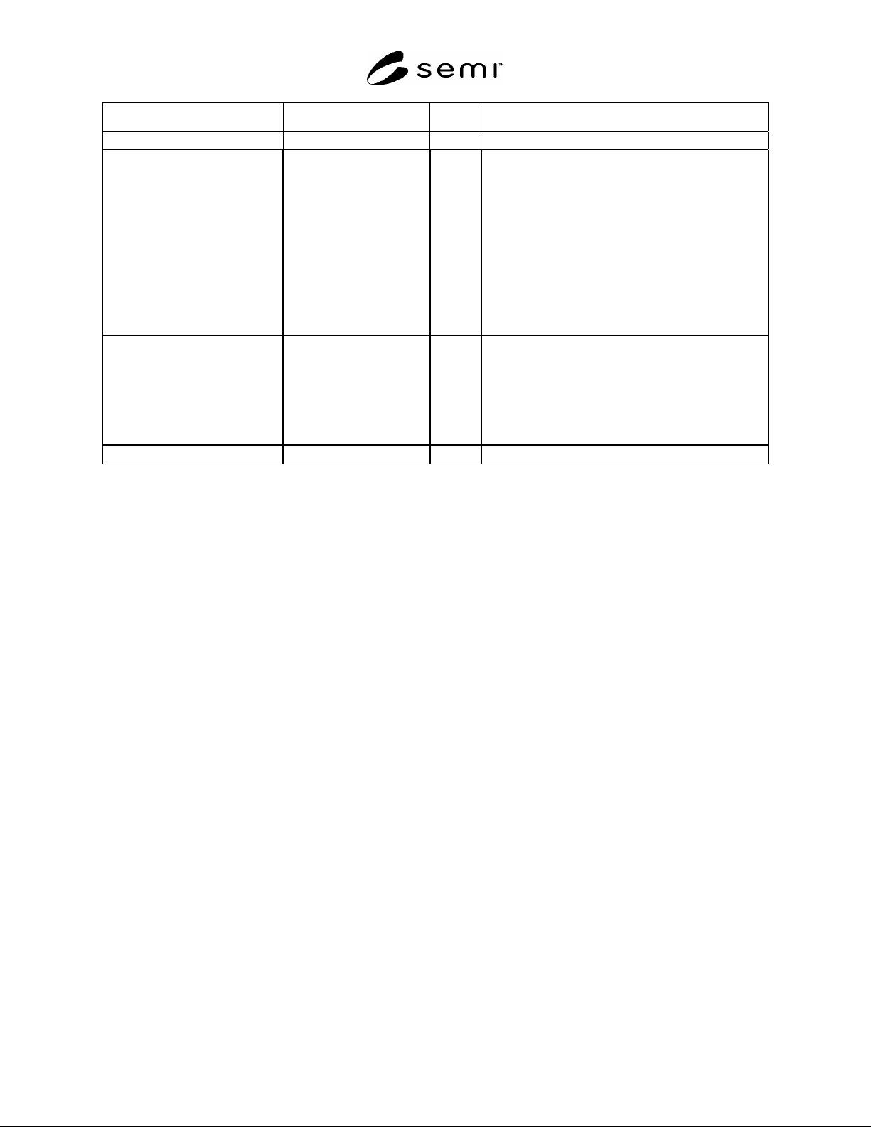
Table 4 Laser Marking Requirements (see Figure 8 of SEMI M55)
Property Dimension Units
GEOMETRY
dimension A 0.5 mm
dimension B 2.0 mm
dimension C 10.0 mm
#1
MARKING DEPTH
100
µm target value 30µm
CHARACTER SET Defined by SEMI M12 character font and proportions (“SEMI OCR”), not
font size
CHARACTER DIMENSIONS
Option 1: “large”
#3, #4
dimensions according to SEMI M12, readable with
unaided eye
Character Height
1.624 0.025
mm
Character Spacing
1.420 0.025
mm
width and thickness are defined by the proportions
given in SEMI M12
Option 2: “small”
#2, #4
dimensions according to SEMI M13, readable with
unaided eye
Character Height
0.812 0.025
mm
Character Spacing
0.710 0.025
mm
width and thickness are defined by the proportions
given in SEMI M13
SEMI M55.2-0705 © SEMI 2005 4
Property Dimension Units
FORMAT OF ID-STRING
Option 1:”OCR Checksum
Character”
#2, #4
NNNNNNNNNNSSCC
(14 characters total)
NNNNNNNNNN: (10 characters)
supplier defined ID of wafer, with a dash as
separator. Unused characters are filled with dash
characters. Alphanumeric.
SS: (2 characters)
Supplier Identification Code as defined in SEMI
AUX1. Alpha only.
CC: (2 characters)
Checksum Characters generated by the algorithm
defined in SEMI M12.
The first character is alpha only, the second
numeric only.
Option 2: “manual reading”
#3, #4
NNNNSS to
NNNNNNNNNNSS
(6 to 12 characters total)
NNNNNNNNNN: (4 to 10 characters)
supplier defined ID of wafer, with a dash as
separator. Alphanumeric with a dash as fill
character.
SS: (2 characters)
Supplier Identification Code as defined in SEMI
AUX1. Alpha only.
#1
The total width of the marking window is twice dimension C.
#2
Option is intended for use with automated systems including OCR-techniques.
#3
Option is intended primarily for manual reading of the wafer ID and allows shorter ID-strings which are preferable for manual reading. A
Supplier Identification Code is mandatory as the last two characters.
#4
Size and format options may be used in any combination.
NOTICE: SEMI makes no warranties or representations as to the suitability of the standards set forth herein for any
particular application. The determination of the suitability of the standard is solely the responsibility of the user.
Users are cautioned to refer to manufacturer’s instructions, product labels, product data sheets, and other relevant
literature, respecting any materials or equipment mentioned herein. These standards are subject to change without
notice.
By publication of this standard, Semiconductor Equipment and Materials International (SEMI) takes no position
respecting the validity of any patent rights or copyrights asserted in connection with any items mentioned in this
standard. Users of this standard are expressly advised that determination of any such patent rights or copyrights, and
the risk of infringement of such rights are entirely their own responsibility.
Copyright by SEMI® (Semiconductor Equipment and Materials
International), 3081 Zanker Road, San Jose, CA 95134. Reproduction of
the contents in whole or in part is forbidden without express written
consent of SEMI.