semi合集-English.pdf - 第5359页
SEMI M53-1103 © SEMI 2003 10 R1-1.5 The accuracy of the peak diameter, which is specified to have a relative exp anded uncertainty at about 95% confidence level as small as possible but not greater than 3% in SEMI M52, i…

SEMI M53-1103 © SEMI 2003 9
RELATED INFORMATION 1
DEPOSITION ISSUES
NOTICE: This related information is not an official part of SEMI M53 and was derived from the work of the
Automated Wafer Surface Inspection Task Force. This related information was approved for publication by full
letter ballot on November 22, 2002.
R1-1.1 Both this practice and SEMI M52 introduce the
notion that SSIS calibration should depend on the
characteristics of PSL sphere depositions as they appear
on the reference wafers, rather than the previous
technique of using the bulk characteristics of the PSL
spheres measured prior to being deposited. This change
in philosophy has come about for two reasons. First, in
many situations, there is actually some advantage to
creating depositions with different characteristics from
those of the bulk PSL spheres. For example, the
deposition process may be used to narrow the diameter
distribution thus creating a standard that more closely
approximates a source of particles of a single known
size. Secondly, most deposition systems produce at
least minor changes in diameter distributions that are
difficult to eliminate in any case. As a result, this
philosophical change is being introduced to increase the
accuracy with which SSIS calibration can be
accomplished.
R1-1.2 Deposition systems generally consist of an
atomizer (which takes the particles from a liquid
suspension to an air droplet mist), followed by a dryer
(so that droplets of the source liquid do not reach the
wafer), and often include a bipolar charger and
differential mobility analyzer (or DMA) to size and/or
filter the particles. The changes in characteristics from
source to deposition are due to at least three distinct
causes. First, virtually all atomizers bias the diameter
distribution slightly in favor of smaller particles. This
is because the larger particles do not “fit” in the smaller
droplets and as a result have a smaller probability of
ending up in the airborne stream of particles headed
towards the wafer. For narrow source distributions this
is not much of an issue, but for wider source
distributions it is. Secondly, the source liquid often
contains non-volatile solids that may dry onto the
particles, thus slightly changing their diameter.
Although this is not as important for larger particles
greater than 200 nm, it is highly recommended that a
PSL suspension with low non-volatiles be used to
reduce this source of error. If the DMA is operated in a
manner that meets the requirement of this practice for
distributions with full width at half maximum (FWHM)
of no more than 5% of the peak diameter, then many
source distributions are narrowed by the DMA. This is
true because many PSL sphere sources with diameters
less than 200 nm have FWHM values wider than 5% of
peak value. The 5% FWHM value does not impose
severe difficulties on the DMA design.
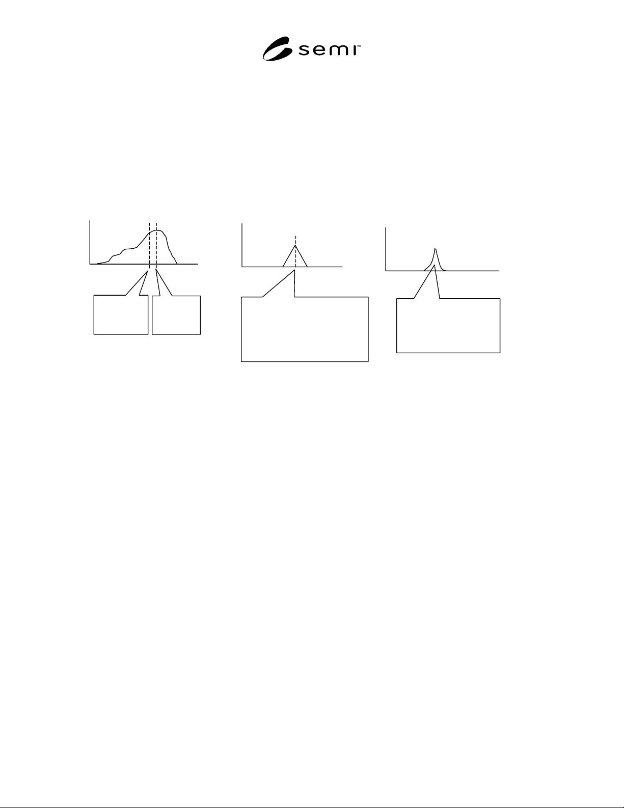
R1-1.3 In addition to narrowing the deposition
diameter distributions, these standards address related
accuracy issues. These are easily understood by
considering the filtering process of the DMA on the
source distribution as shown in Figure R1-1. The left
hand side of the figure represents a rather broad PSL
source diameter distribution. Notice that it is not
symmetrical, which makes the mean (or average)
diameter different from the modal (or peak) diameter.
Typically PSL manufacturers have given the mean
diameter with their product and industry users have
assigned this value as the diameter for that deposition.
Unfortunately depositions are generally made at the
peak diameter. This is because the peak is easily found
by scanning the DMA through the source distribution
while counting the number of particles passing the
DMA. The center section of the figure shows the ideal
triangular transfer function of the DMA fixed at some
center diameter. By adjusting airflows through the
DMA, the FWHM can be changed. By adjusting an
applied voltage, the center pass diameter of the transfer
function can be changed. In effect, the deposition
characteristics are formed through the multiplication of
the transfer function with the source distribution as
indicated on the right hand side of the figure.
R1-1.4 Notice that the shape of the deposition
distribution is triangular with bowed in sides, because
the source distribution is not flat. In effect, this is a
safety factor for the 5% FWHM specification. Because
the source distribution is not necessarily symmetrical,
the deposition distribution may not be either; however,
the mean and peak deposition diameters will be very
close because the distribution is relatively narrow.
SEMI M53-1103 © SEMI 2003 10
R1-1.5 The accuracy of the peak diameter, which is specified to have a relative expanded uncertainty at about 95%
confidence level as small as possible but not greater than 3% in SEMI M52, is determined by either the accuracy
with which the peak source diameter is known (or can be found), or by the accuracy of the DMA sweep
voltage/diameter relationship. Unfortunately many PSL source bottles currently in use do not give the peak
diameter, so this presents a difficulty for the first approach. The second approach, relying on DMA voltage
accuracy, can be checked by using PSL sources that are known to be very narrow (to minimize differences between
source and deposition peak diameter) with very accurate peak values.
PSL Source Diameter
Distribution
Mean, or
average,
diameter
Peak, or
modal,
diamete
Diameter
Counts/Diameter
X =
Deposition Transfer
Function
In many deposition
systems, the transfer
function may be scanned
through the diameter
distribution and set to the
p
eak diameter.
Transmission
Diameter
Deposition Diameter
Distribution
Diameter
Counts/Diameter
The shape of the
deposition diameter
distribution is no
wider than the
transfer function.
Figure R1-1
The Diameter Distribution of the Deposition is the Product of the Deposition System Transfer Function and
the Source (or “Bottle”) Distribution.
NOTICE: SEMI makes no warranties or representations as to the suitability of the standards set forth herein for any
particular application. The determination of the suitability of the standard is solely the responsibility of the user.
Users are cautioned to refer to manufacturer's instructions, product labels, product data sheets, and other relevant
literature, respecting any materials or equipment mentioned herein. These standards are subject to change without
notice.
By publication of this standard, Semiconductor Equipment and Materials International (SEMI) takes no position
respecting the validity of any patent rights or copyrights asserted in connection with any items mentioned in this
standard. Users of this standard are expressly advised that determination of any such patent rights or copyrights, and
the risk of infringement of such rights are entirely their own responsibility.
Copyright by SEMI® (Semiconductor Equipment and Materials
International), 3081 Zanker Road, San Jose, CA 95134. Reproduction o
f
the contents in whole or in part is forbidden without express written
consent of SEMI.

SEMI M54-0304 © SEMI 2003, 2004 1
SEMI M54-0304
GUIDE FOR SEMI-INSULATING (SI) GaAs MATERIAL PARAMETERS
This guide was technically approved by the Global Compound Semiconductor Committee and is the direct
responsibility of the European Compound Semiconductor Materials Committee. Current edition approved by
the European Regional Standards Committee on January 9, 2004. Initially available at www.semi.org
February 2004; to be published March 2004. Originally published March 2003.
1 Purpose
1.1 Substrates with high electrical resistivity and
electron drift mobility are needed to fabricate high
performance digital and analog microelectronic devices
and circuits. Semi-insulating n-type Gallium Arsenide,
henceforth termed SI GaAs, has been established
worldwide as a preferred substrate material for such
applications.
1.2 The active layers needed for devices are generated
either by ion implantation or by epitaxy. The quality of
these layers, and hence the performance, yield and
reliability of devices, strongly depends on the bulk and
surface quality of the substrate.
1.3 This document provides a basis for specifying the
material parameters of SI GaAs to support ordering
agreements between suppliers and purchasers.
2 Scope
2.1 This document defines and describes the electrical,
optical, structural, and surface properties of SI GaAs
that are considered technically relevant according to the
present status of scientific knowledge and material
technology.
2.2 A specification of the material quality of SI GaAs
substrates includes a number of the parameters
described below. Depending on the intended
application, a particular subset of properties and
respective parameters will be considered relevant by the
purchaser.
2.3 In order to enhance the clarity and applicability of
the document, the ordering information in Section 6
subdivides the material parameters in respect of their
relative importance, according to general industry
perception.
2.4 Some material properties and parameters, while
intensively discussed in the technical literature, are
insufficiently established to allow an unambiguous
specification. The available information is nevertheless
included to support supplier-purchaser discussions and
agreements on these issues.
2.5 Each parameter specification requires an agreement
about verification. Appropriate information is
summarized in Section 5. Available standard test
methods elaborated by SEMI, ASTM, and DIN are
referenced in Section 3.
2.6 A number of the required standard test methods do
not exist at present. This document is expected to serve
as a guideline and incentive for qualified ASTM, DIN,
JEITA, and SEMI committees to develop the missing
standard procedures. Conversely, if at present more
than one standard test method for verification of a
specific parameter exists (see Table 1), a global
consensus procedure towards selecting or generating a
unique standard is advocated.
2.7 The geometrical properties of wafers, in particular
orientation, diameter, thickness, flatness and edge
rounding, are covered by the series of SEMI M9
specifications and shall not be addressed here.
NOTICE: This standard does not purport to address
safety issues, if any, associated with its use. It is the
responsibility of the users of this standard to establish
appropriate safety and health practices and determine
the applicability of regulatory or other limitations prior
to use.
3 Referenced Standards
3.1 SEMI Standards
SEMI M9 — Specifications for Polished
Monocrystalline Gallium Arsenide Slices
SEMI M10 — Standard Nomenclature for
Identification of Structures and Features Seen on
Gallium Arsenide
SEMI M15 — Polished Wafer Defect Limits Table for
Polished Gallium Arsenide Wafers
SEMI M30 — Standard Test Method for Substitutional
Atomic Carbon Concentration in GaAs by Fourier
Transform Infrared Absorption
SEMI M36 — Test Method for Measuring Etch Pit
Density (EPD) in Low Dislocation Density Gallium
Arsenide Wafers
SEMI M39 — Test Method for Measuring Resistivity
and Hall Coefficient and Determining Hall Mobility in
Semi-insulating GaAs Single Crystals