semi合集-English.pdf - 第4879页
SEMI M2-1103 © SEMI 1985, 2003 5 Table 1 Discrete Epitaxial Wafer Defect Li mits Item Characteristics Maximu m Limit Test Method Notes 1 Stacking Faults 15 per cm 2 SEMI MF1726 1 2 Slip n = 36 grid elements SEMI M17 and …
SEMI M2-1103 © SEMI 1985, 2003 4
9 Certification
9.1 Upon request of the purchaser in the contract or
order, a manufacturer’s or supplier’s certification that
the material was manufactured and tested in accordance
with this specification, together with a report of the test
results, shall be furnished at the time of shipment.
9.2 The user and supplier may agree that the material
shall be certified as “capable of meeting” certain
requirements. In this context, “capable of meeting”
shall signify that the supplier is not required to perform
the appropriate tests in Section 8; however, if the user
performs the test and the material fails to meet the
requirement, the material may be subject to rejection.
10 Packing and Package Labeling
10.1 Special packing requirements shall be subject to
agreement between the supplier and the purchaser.
Otherwise, all wafers shall be handled, inspected, and
packed in such a manner as to avoid chipping,
scratches, and contamination, and in accordance with
the best industry practices to provide protection against
damage during shipment.
10.2 The wafers supplied under these specifications
shall be identified by appropriately labeling the outside
of each box or container, and each subdivision thereof,
in which it may reasonably be expected that the wafers
will be stored prior to further processing. Identification
shall include supplier’s name and reference number,
purchaser’s P.O. number, quantity, dopant, orientation,
conductivity type of substrates and epitaxial layers,
carrier density (or resistivity, if so specified in the
purchase order or contract), and thickness of the
epitaxial layer. The reference number assigned by the
supplier shall provide ready access to information
concerning the fabrication history of the particular
wafers in that lot. Such information shall be retained on
file at the manufacturer’s facility for at least one year
after the particular lot has been shipped.
SEMI M2-1103 © SEMI 1985, 2003 5
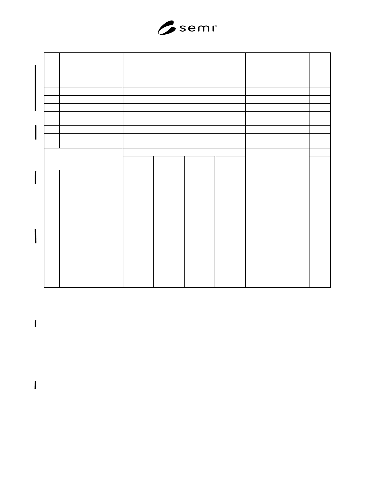
Table 1 Discrete Epitaxial Wafer Defect Limits
Item Characteristics Maximum Limit Test Method Notes
1 Stacking Faults 15 per cm
2
SEMI MF1726 1
2 Slip n = 36 grid elements SEMI M17 and SEMI
MF1726
1, 2, 3
3 Haze NONE SEMI MF523 Section 12.2 1, 4, 5
4 Scratches NONE SEMI MF523 Section 12.2 1, 5, 6
5 Edge Chips NONE SEMI MF523 Section 12.2 7
6 Edge Crown Projection above wafer surface not to exceed 1/3 of
epi layer thickness
To be defined 2, 8
7 Foreign Matter NONE SEMI MF523 Section 12.3 1, 4
8 Back Surface
Contamination
NONE SEMI MF 523 Section 12.4 1, 4
Epitaxial Layer Thickness Front Surface
Characteristics Dependent on
Layer Thickness
< 25 µm 25–50 µm 50–100 µm > 100 µm
9 Large Point Defects
(Density per m
2
)
700 900 1200 1500 SEMI MF523 or, with
automated surface
inspection equipment
≥ 20 µm LSE, based on
calibration of surface
scanning inspection
systems with polystyrene
latex spheres, 90% capture
rate
1, 2, 5
10 Total Localized Light
Scatterers
(Density per m
2
)
2000 2400 2700 3000 SEMI MF523 or with
automated surface
inspection equipment
≥ 0.5 µm LSE, based on
calibration of surface
scanning inspection
systems with polystyrene
latex spheres, 90% capture
rate
1, 2, 5
Notes:
1. Defect limits shall apply to quality area, which is defined as the entire wafer surface except a defined outer annulus: 2 inch and 3 inch = 2 mm;
100 mm and 125 mm = 3 mm; 150 mm and 200 mm = 4 mm and any are included in a window where there is a laser indentification mark.
2. Test method(s) to be agreed upon between supplier and purchaser.
3. For observation of gross slip, examine the epi layer under illumination conditions specified in Section 12.2 of SEMI MF523. For more
demanding applications, it may be desirable to etch the surface in accordance with SEMI MF1726 prior to the visual inspection.
4. Any adherent contaminants, such as stains, glovemarks, dirt, smudges, and solvent residues. This characteristic does not include point defects.
Any nonadherent contaminant or particulate matter easily removed by industry accepted cleaning techniques shall not constitute foreign matter or
haze.
5. In today’s technology, it may be possible to do this inspection using automated laser scanning systems; however, a standard test procedure has
yet to be developed. Application of automated inspection must be agreed upon between supplier and user.
6. The cumulative AQL for both front surface and back surface of wafer is 2.5%.
7. The cumulative AQL for both front surface and back surface of wafer is 1.0%. Maximum radial penetration, 1.0 mm; maximum single chip
peripheral length, 6.3 mm; maximum cumulative peripheral length, 6.3 mm.
8. Edge crowning may be reduced by pre-epitaxy edge rounding, or removed by post-epitaxy edge rounding.

SEMI M2-1103 © SEMI 1985, 2003 6
NOTICE: SEMI makes no warranties or representations as to the suitability of the standards set forth herein for any
particular application. The determination of the suitability of the standard is solely the responsibility of the user.
Users are cautioned to refer to manufacturer’s instructions, product labels, product data sheets, and other relevant
literature respecting any materials mentioned herein. These standards are subject to change without notice.
The user’s attention is called to the possibility that compliance with this standard may require use of copyrighted
material or of an invention covered by patent rights. By publication of this standard, SEMI takes no position
respecting the validity of any patent rights or copyrights asserted in connection with any item mentioned in this
standard. Users of this standard are expressly advised that determination of any such patent rights or copyrights, and
the risk of infringement of such rights, are entirely their own responsibility.
Copyright by SEMI® (Semiconductor Equipment and Materials
International), 3081 Zanker Road, San Jose, CA 95134. Reproduction o
f
the contents in whole or in part is forbidden without express written
consent of SEMI.