semi合集-English.pdf - 第41页
SEMI E1.9-0701 E2 © SEMI 1994, 2004 21 Table A1-1 Open Cassette Option al Features Checklist Section Optional Feature Choice 6.9 carrier capacity (c) 13 wafers or 25 wafers 6.7.4 slant on 2 required fork-lift pick-up are…
SEMI E1.9-0701
E2
© SEMI 1994, 2004 20
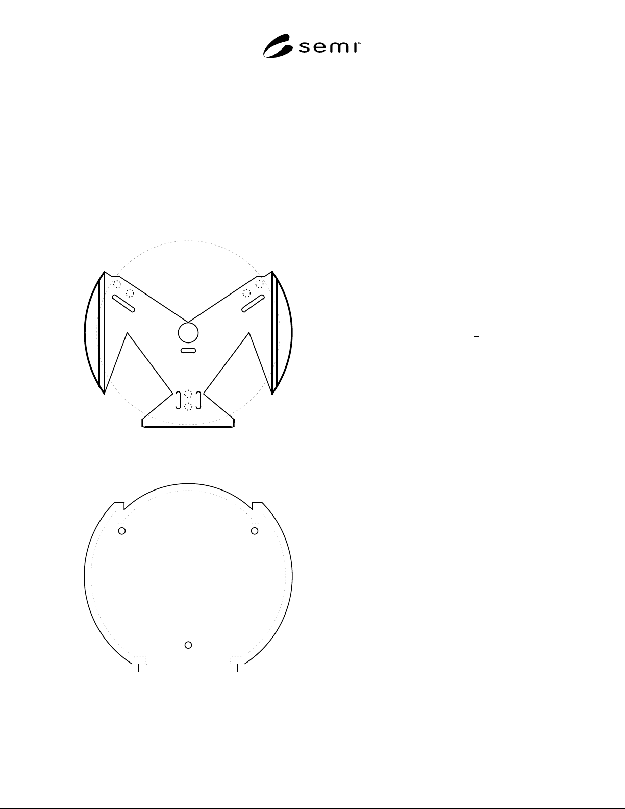
A1-9 Figure A1-3 shows a small-footprint cassette that
conforms to the requirements of this specification. In
order to prevent such a small cassette from being set on
the kinematic couplings in the wrong orientation, a
frame such as shown in Figure A1-4 can be placed
around the couplings. In order to not interfere with the
kinematic couplings alignment function, the frame can
extend no further than r19 from the maximum
boundaries of a cassette.
NOTE: If the bottom of the cassette does not extend below
the bottom conveyor rail, the conveyor rail may become
contaminated and may distribute particles.
Figure A1-3
Small-Footprint Cassette
Figure A1-4
Frame to Prevent Misalignment
A1-10 Conveyor rail edges need to be well defined for
smooth guidance and to avoid vibration. Thus, the
minimum radius on the edge that does not create
particles is recommended. For similar reasons, the
tolerance on conveyor rail parallelism and on
dimension x16 should be kept as small as possible for
the materials used.
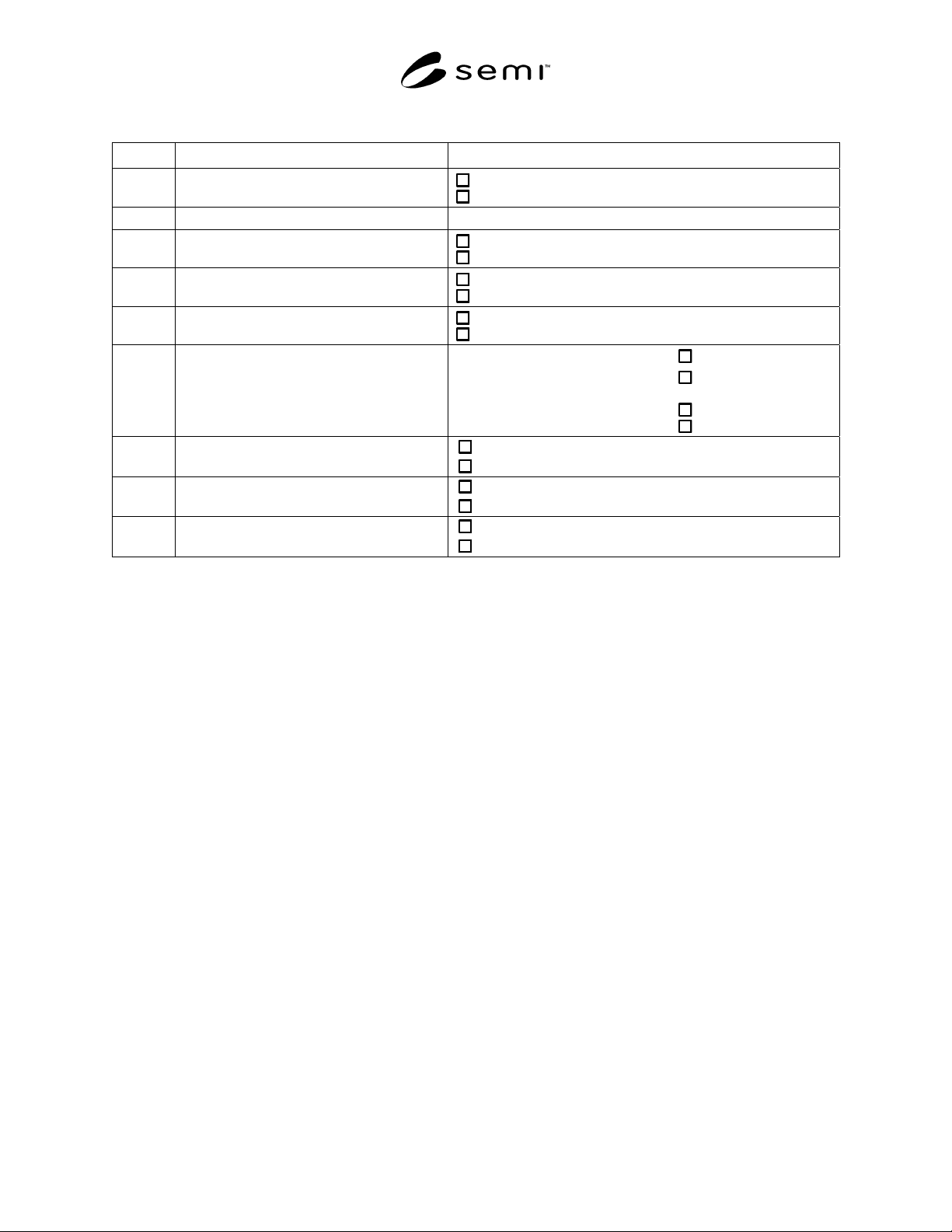
A1-11 Table A1-1 can be used for communicating
which optional features are present on cassettes that
comply with this specification.
A1-12 In general, info pad A (on the lower left in
Figure 5) was intended to indicates
the carrier capacity
(the number of wafers). For example, info pad A was
previously defined to be in the down position (at z2
above horizontal datum plane) if the carrier holds 13
wafers and was previously defined to be in the up
position (at z26 above horizontal datum plane) if the
carrier holds 25 wafers. Info pad A is intended to be
read with a mechanical switch or optical sensor.
A1-13 In general, info pad B (on the lower right in
Figure 5) was intended to indicates
the carrier type
(cassette or box, etc.). For example, info pad B was
previously defined to be in the down position (at z2
above horizontal datum plane) if the carrier is a cassette
and was previously defined to be in the up position (at
z26 above horizontal datum plane) if the carrier is a
box. Info pad B is intended to be read with a
mechanical switch or optical sensor.
A1-14 Info pads C and D (slightly forward and to the
outside of info pads A and B) are intended to show
whether the carrier is dedicated to the front-end-of-line
(FEOL) part of the fabrication process (before any
metal layers have been deposited on the wafer) or to the
back-end-of-line (BEOL) part of the fabrication process
(during which metal contamination may be present). If
such carrier differentiation is required by the user, info
pads C and D are recommended to be down and up
(respectively) for a front-end-of-line carrier and the
opposite for a back-end-of-line carrier. Info pads C and
D are intended to interact with a mechanical pin. See
application note R1-2 in SEMI 15.1 for a discussion of
how to use pins to differentiate FEOL and BEOL
carriers.
SEMI E1.9-0701
E2
© SEMI 1994, 2004 21
Table A1-1 Open Cassette Optional Features Checklist
Section Optional Feature Choice
6.9 carrier capacity (c)
13 wafers or
25 wafers
6.7.4 slant on 2 required fork-lift pick-up areas
angle ω = ____ (0° ≤ ω ≤ 2°)
6.4 4 robotic handling flanges
yes or
no
6.3 4 pentagonal side grip pits
yes or
no
6.7.1 features that prevent wafer creep-out
yes or
no
6.1 full 15 mm lead in provided by 3 features
that mate with kinematic coupling pins
primary kinematic coupling pins
yes or
no
and
secondary kinematic coupling pins
yes or
no
6.8.1 top cassette identification tag area
yes or
no
6.8.3 bottom cassette identification tag area
yes or
no
6.8.2 side cassette identification tag area (on front
right side domain)
yes or
no
NOTICE: These standards do not purport to address safety issues, if any, associated with their use. It is the
responsibility of the user of these standards to establish appropriate safety and health practices and determine the
applicability of regulatory limitations prior to use. SEMI makes no warranties or representations as to the suitability
of the standards set forth herein for any particular application. The determination of the suitability of the standard is
solely the responsibility of the user. Users are cautioned to refer to manufacturer' s instructions, product labels,
product data sheets, and other relevant literature respecting any materials mentioned herein. These standards are
subject to change without notice.
The user' s attention is called to the possibility that compliance with this standard may require use of copyrighted
material or of an invention covered by patent rights. By publication of this standard, SEMI takes no position
respecting the validity of any patent rights or copyrights asserted in connection with any item mentioned in this
standard. Users of this standard are expressly advised that determination of any such patent rights or copyrights, and
the risk of infringement of such rights are entirely their own responsibility.

SEMI E1.9-0701
E2
© SEMI 1994, 2004 22
RELATED INFORMATION 1
NOTE: This related information is not an official part of
SEMI E1.9, and it is not intended to modify or supersede the
standard in any way. This information was inserted by the
North America Physical Interfaces and Carriers Committee to
alert the readers to potential changes to this provisional
standard.
R1-1 A revision ballot will be submitted to insert a
statement that application of info pads C and D are
reserved to be defined by the user (for example,
distinguishing between FEOL and BEOL carriers).
NOTICE: These standards do not purport to address
safety issues, if any, associated with their use. It is the
responsibility of the user of these standards to establish
appropriate safety and health practices and determine
the applicability of regulatory limitations prior to use.
SEMI makes no warranties or representations as to the
suitability of the standards set forth herein for any
particular application. The determination of the
suitability of the standard is solely the responsibility of
the user. Users are cautioned to refer to manufacturer' s
instructions, product labels, product data sheets, and
other relevant literature respecting any materials
mentioned herein. These standards are subject to
change without notice.
The user' s attention is called to the possibility that
compliance with this standard may require use of
copyrighted material or of an invention covered by
patent rights. By publication of this standard, SEMI
takes no position respecting the validity of any patent
rights or copyrights asserted in connection with any
item mentioned in this standard. Users of this standard
are expressly advised that determination of any such
patent rights or copyrights, and the risk of infringement
of such rights are entirely their own responsibility.
Copyright by SEMI® (Semiconductor Equipment and Materials
International), 3081 Zanker Road, San Jose, CA 95134. Reproduction o
f
the contents in whole or in part is forbidden without express written
consent of SEMI.