semi合集-English.pdf - 第4992页
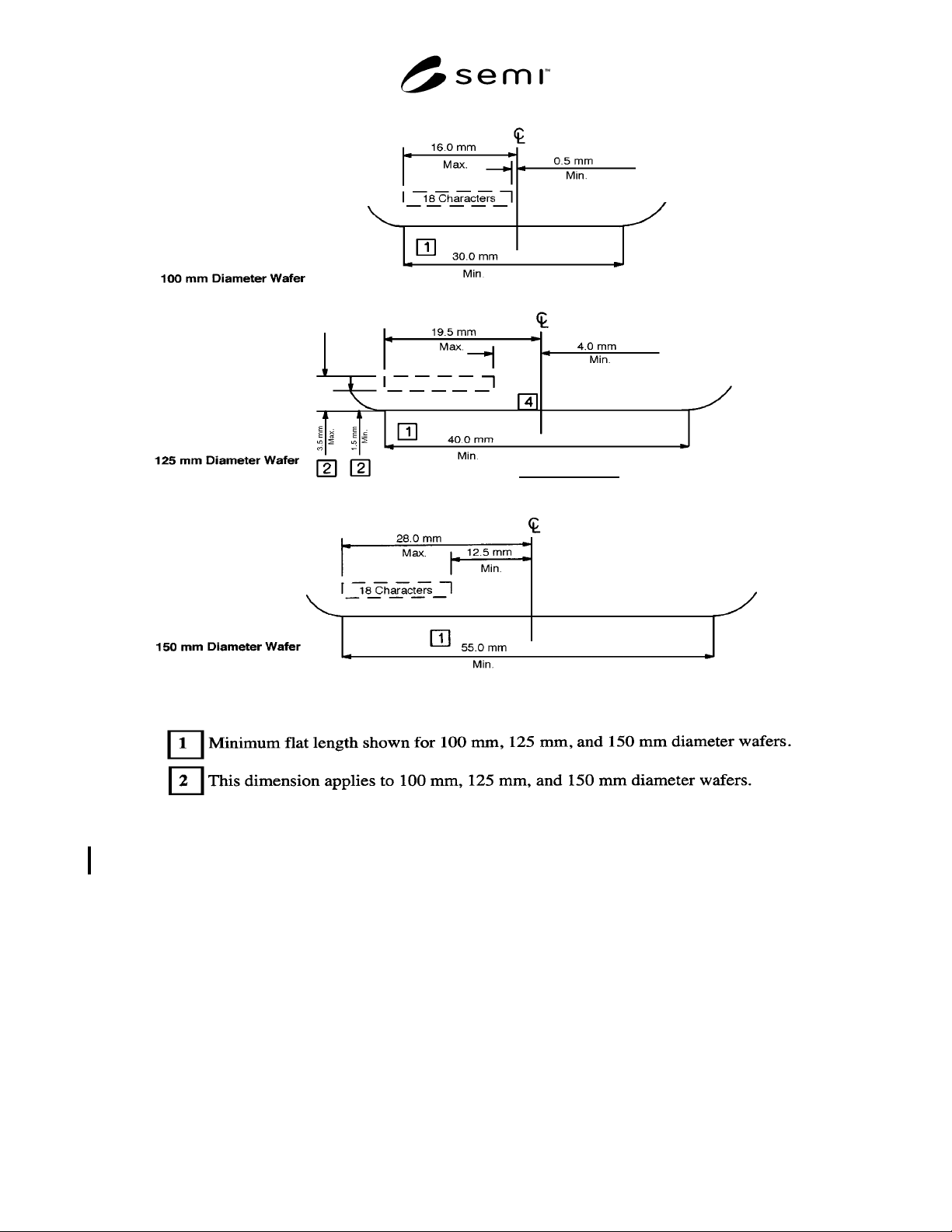
SEMI M13-1103 © SEMI 1988, 2003 4 Figure 3 Code Field Locati on for Flatted Wafers
SEMI M13-1103 © SEMI 1988, 2003 3
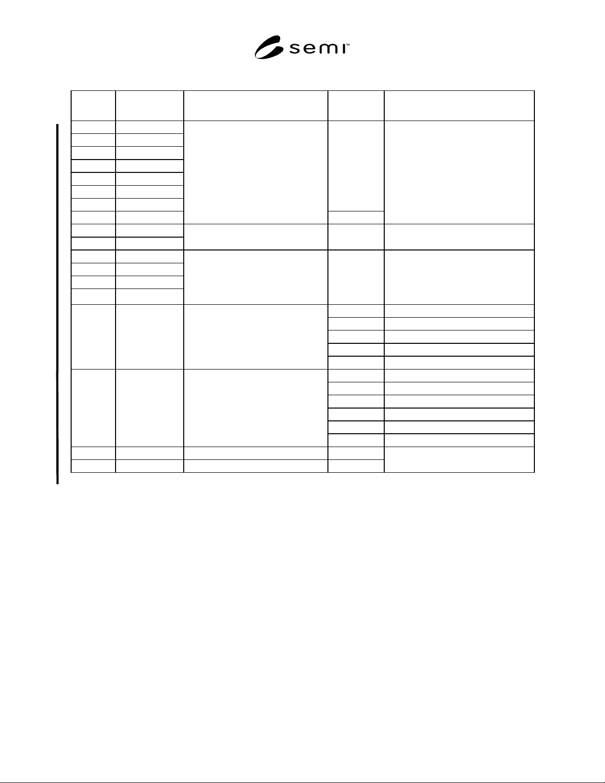
Table 3 Code
Character
Location
CharacterStyle Parameter Code Definition
1 Alpha/Numeric
2 Alpha/Numeric
3 Alpha/Numeric
4 Alpha/Numeric
5 Alpha/Numeric
6 Alpha/Numeric
7 Alpha/Numeric
A through Z
and
0 through 9
8 Numeric Only
IDENTIFICATION NUMBER
0 through 9
Supplier-Assigned (See NOTE 1.)
9 Alpha Only
10 Alpha Only
SUPPLIER IDENTIFICATION A through Z (see SEMI AUX001 and NOTE 1.)
11 Numeric Only
12 Numeric Only
13 Numeric Only
14 Numeric Only
RESISTIVITY IDENTIFICATION
0 through 9
and .(period)
Resistivity (Ω·cm) identification is
assigned by supplier, expressed as a
whole number or as a mixed number
with a decimal fraction. No accuracy is
implied. (See NOTE 1.)
B Boron
F Phosphorous
A Arsenic
S Antimony
15 Alpha Only DOPANT SPECIES
– not identified
0 [100]
1 [111]
2 [110]
3 [011]
5 [511]
16
Numeric Only
CRYSTAL GROWTH
ORIENTATION
– not identified
17 Alpha Only CHECK CHARACTER A
17
A through H
18 Numeric Only CHECK CHARACTER A
18
0 through 7
Error-Detecting Method
(see Section 7)
NOTE 1: In the absence of information at any assigned location, a dash (–) must be used.
SEMI M13-1103 © SEMI 1988, 2003 4
Figure 3
Code Field Location for Flatted Wafers
SEMI M13-1103 © SEMI 1988, 2003 5
max
min
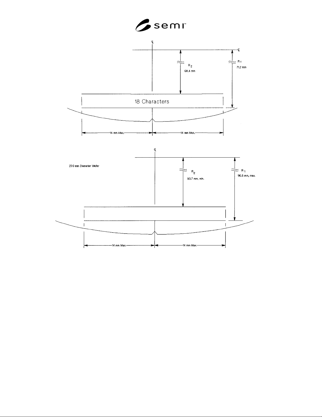
Figure 4
Field Location for Notched Wafers