semi合集-English.pdf - 第6531页
SEMI G81-0703 © SEMI 2000, 2003 6 ReferenceDeviceX="4" ReferenceDeviceY="-5" RefDevicePosX="2" RefDevicePosY="2" /> <Bin BinCode="02" BinQuality="Pass" Bi…
SEMI G81-0703 © SEMI 2000, 2003 5
Item Name Data Type Size Description
CreateDate String 16 Date and time when the map data is acquired: formatted as YYYYMMDDhhmmsscc
(year-month-date-hour-minute-second-centisecond).
Status String 16 Status of map data supplying process or preceding process.
Label String 256 Name of a special parameter.
SupplierValue String 256 Value of a special parameter.
SlotNumber Integer 2 This identifies the slot in the carrier in which the substrate is placed.
SubstrateNumber Integer 2 Identifies the substrate within a lot.
GoodDevices Integer 4 The total number of “good” devices on the substrate. The definition of “good” is
beyond the scope of this document.
SubstrateType String 16 The type of substrate. The choices are as follows:
[SubstrateType] = ‘Wafer’
[SubstrateType] = ‘Strip’
[SubstrateType] = ‘Tray’
SubstrateId String 32 A character code that may be printed or encoded on the substrate, which uniquely
identifies the substrate, and can be used to correlate the map with the physical
substrate.
CarrierType String 16 The type of substrate carrier. The choices are as follows:
[CarrierType] = ‘Cassette’
[CarrierType] = ‘Magazine’
CarrierId String 32 A character code that may be printed or encoded on the substrate carrier, which
uniquely identifies the substrate carrier.
LastModified String 16
Date and time when the map data was last modified: formatted as
YYYYMMDDhhmmsscc (year-month-date-hour-minute-second-centisecond)
NOTE 1: A set of above items is prepared for each single substrate to make it possible to consolidate more than one lot in a cassette.
7.3 Example
<?xml version="1.0"?>
<Map xmlns=”http://www.semi.org” SubstrateType=”Wafer”
SubstrateId="ZSDGS88DF" FormatRevision="SEMI G85-0703">
<Device
ProductId="854CS1C"
LotId="wksfd87dcj37"
Orientation="0"
DeviceSizeX="343.8"
DeviceSizeY="373.1"
Rows="6"
Columns="6"
BinType="HexaDecimal"
FrameId="KJKSDFK45"
NullBin="FF"
SupplierName="Company X"
OriginLocation="1"
CreateDate="2002110112000000"
LastModified="2003010612000000"
Status="Product">
<ReferenceDevice
ReferenceDeviceX="2"
ReferenceDeviceY="-3"
RefDevicePosX="2"
RefDevicePosY="2"
/>
<ReferenceDevice

SEMI G81-0703 © SEMI 2000, 2003 6
ReferenceDeviceX="4"
ReferenceDeviceY="-5"
RefDevicePosX="2"
RefDevicePosY="2"
/>
<Bin
BinCode="02"
BinQuality="Pass"
BinDescription="500MHz"
/>
<Data MapName="SortGrade" Version="1">
<Row><![CDATA[FFFF020CFFFF]]></Row>
<Row><![CDATA[FF14020C02FF]]></Row>
<Row><![CDATA[0202020C0116]]></Row>
<Row><![CDATA[0201140C0202]]></Row>
<Row><![CDATA[FF14020C02FF]]></Row>
<Row><![CDATA[FFFF020CFFFF]]></Row>
</Data>
</Device>
</Map>
SEMI G81-0703 © SEMI 2000, 2003 7
APPENDIX 1
WAFER MAP
NOTICE: The material in this appendix is an official part of SEMI G81 and was approved by full letter ballot
procedures on August 27, 2001.
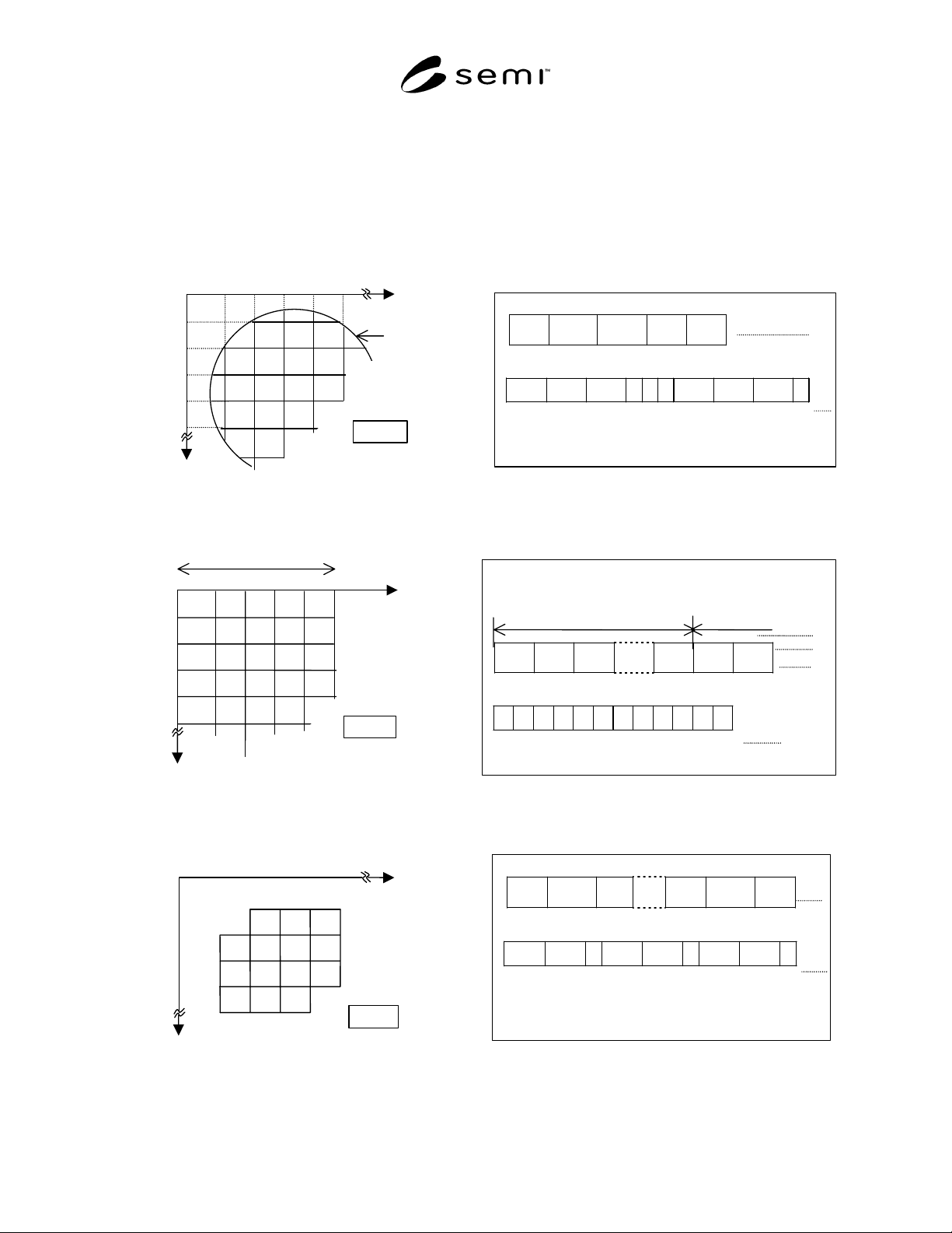
A1-1 This appendix shows how the map data items may be applied to wafers as well as some additional information
specific to this substrate type. See Figures A1-1 through A1-8.
ORIGIN
Column
Row
0
1234
0
1
2
3
4
WAFER
3
3
3
31
1
1
1
NUMBER:BIN DATA
2
2
2
2
2
2
DATA STRUCTURE
Col.
Row.
CHIP
QTY.
Bin Bin
DATA EX.
0002 0001 0003 3 1 3 0001 0002 0004 3
1
Figure A1-1a
Row/Column Format (MapType = “Row”)
ORIGIN
Column
Row
01 234
0
1
2
3
4
3
2
3
31
1
1
1
NUMBER:BIN DATA
2
2
2
2
2
2
DATA STRUCTURE
Bin
Bin Bin … Bin Bin Bin
DATA EX.
000000031303
1
COLUM NUMBER=5
00
00
0
00
0
0
0
Row=0
Col=0 Col=1 Col=2 Col=0
Col=1
Col=n
Row=1
Figure A1-1b
Array Format (MapType = “Array”)
Row
01234
0
1
2
3
4
1
1
1
1
NUMBER:BIN DATA
2
2
22
2
2
DATA STRUCTURE
Col.
Row. Bin … Col. Row. Bin
DATA EX.
0002 0001 3 0003 0001 1 0004 0001 2
Column
ORIGIN
3
3
2
3
Figure A1-1c
Coordinate Format (MapType = “Device”)