semi合集-English.pdf - 第6233页
SEMI G46-88 © SEMI 1988 10 NOTICE: T hese standards do n ot purport to address safety issues, if any, as sociated with their us e. It is the responsibility of the user of these sta ndards to establish appropriate safety …
SEMI G46-88 © SEMI 19889
V = 5.0 v
T = 400 ms
I = 1.0 mA
t = 20
CU = 249 mV/A
σ
= 53.5 mV/A
CU = 302.5 mV/A
H
H
M
MD
cu
high
limit
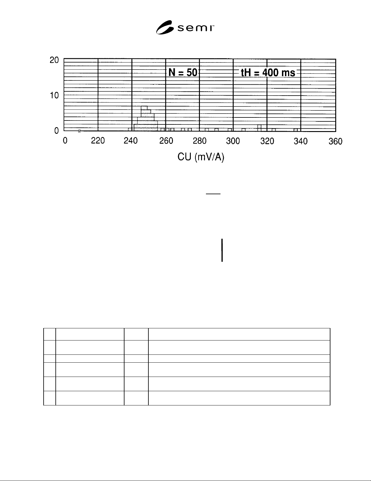
Figure 8
CU bar graph shows thermal distribution of 50 devices when tested at a heating time of 400 ms. (Note: CU data
rounded off to nearest m V/A.)
General Description Steps Comments
A Initial Setup 1 thru 4 Approximate instrument settings to find variations among devices in 10 to 15
piece sample.
B Heating Curve Generation 5 thru 7 Using highest and lowest reading devices, generate Heating Curves.
C Heating Curve Interpretation 8 thru 10 Heating Curve is used to find more appropriate value for t
H
corresponding to heat
in the die attachment are (or some other desired interface in the heat flow path).
D Final Setup 11 Heating Power applied during t
H
is increased in order to improve measurement
sensitivity to variations among devices.
E Pass/F Determination 12 thru 13 A variety of methods is available for setting the fail limit; the statistical approach
is the fastest and easiest to implement.
Figure 9 — Summary table of steps required to implement thermal transient testing for IC die attachment
evaluation.

SEMI G46-88 © SEMI 1988 10
NOTICE: These standards do not purport to address
safety issues, if any, associated with their use. It is the
responsibility of the user of these standards to establish
appropriate safety and health practices and determine
the applicability of regulatory limitations prior to use.
SEMI makes no warranties or representations as to the
suitability of the standards set forth herein for any
particular application. The determination of the
suitability of the standard is solely the responsibility of
the user. Users are cautioned to refer to manufacturer’s
instructions, product labels, product data sheets, and
other relevant literature respecting any materials
mentioned herein. These standards are subject to
change without notice.
The user’s attention is called to the possibility that
compliance with this standard may require use of
copyrighted material or of an invention covered by
patent rights. By publication of this standard, SEMI
takes no position respecting the validity of any patent
rights or copyrights asserted in connection with any item
mentioned in this standard. Users of this standard are
expressly advised that determination of any such patent
rights or copyrights, and the risk of infringement of such
rights, are entirely their own responsibility.
Copyright by SEMI® (Semiconductor Equipment and Materials
International), 3081 Zanker Road, San Jose, CA 95134. Reproduction o
f
the contents in whole or in part is forbidden without express written
consent of SEMI.
SEMI G47-88 © SEMI 19881
SEMI G47-88
SPECIFICATION FOR PLASTIC MOLDED QUAD FLAT PACK
LEADFRAMES
1 Preface
This specification defines the acceptance criteria for
leadframes designed for assembly of JEDEC registered
publication 95 standard outlines for “Plastic Quad Flat
Pack 0.025" lead spacing (gull wing) packages”. It is a
design guideline for packaging engineers, leadframe
stampers and etchers, mold and trim/form tooling
manufacturers. It has been developed to meet the
requirements of assemblers using automatic and manual
equipment.
2 Applicable Documents
2.1 SEMI Specifications
SEMI G4 — Specification, Integated Circuit Leadfame
Materials in the Production of Stamped Frames
SEMI G18 — Specification, Integrated Circuit
Leadframe Materials Used in the Production of Etched
Frames
SEMI G10 — Standard Method, Mechanical
Measurement for Plastic Package Leadframes
SEMI G21 — Specification, Plating Integrated Circuit
Leadframes
2.2 ANSI Specification
1
Y 14.5M-1982 — Dimensioning and Tolerancing
2.3 JEDEC Specification
2
Registration 95 — Plastic Quad Flat Pack, 0.025" Lead
Spacing (Gull Wing)
2.4 Military Specification
3
MIL-STD-105 — Sampling Procedures and Tables for
Inspection by Attributes
3 Selected Definitions
burr — a fragment of excess material either horizontal
or vertical attached to the leadframe.
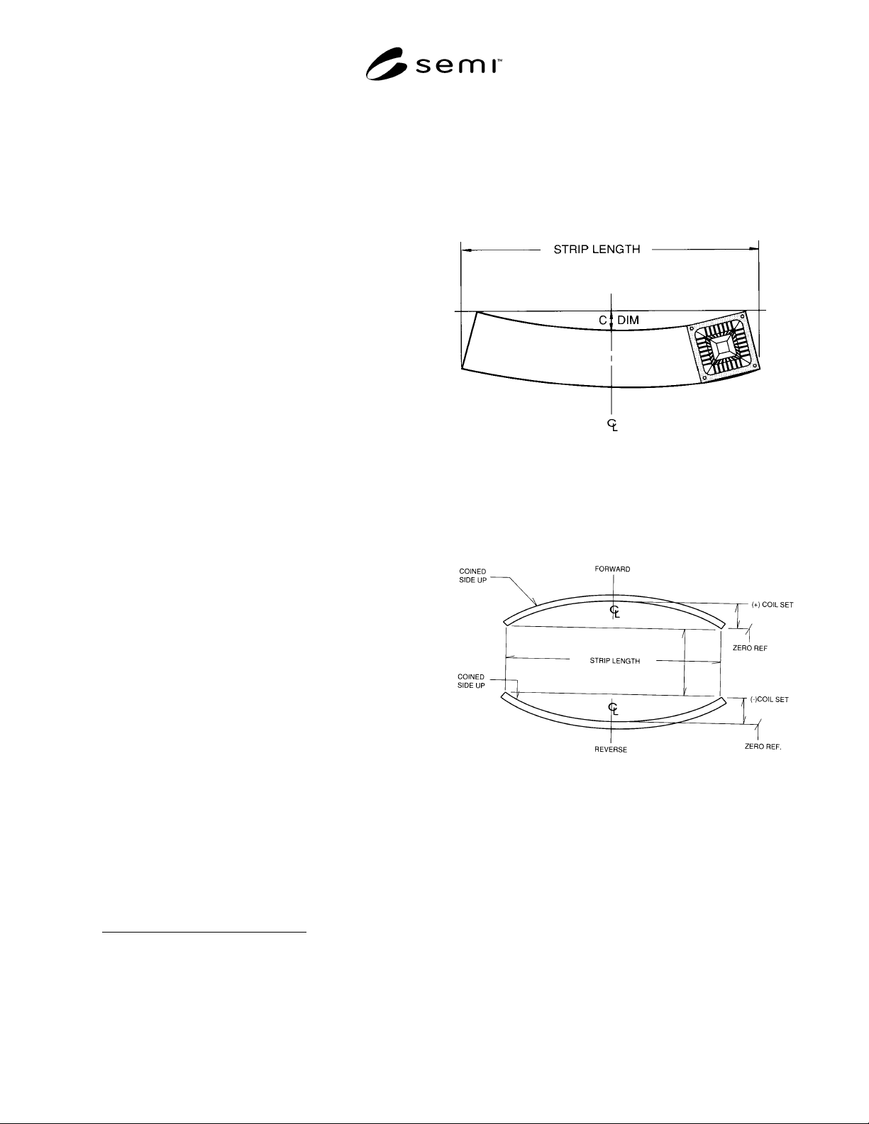
camber — curvature of the leadframe strip edge (see
Figure 1).
1 ANSI, 1430 Broadway, New York, NY 10018
2 Military Standards, Naval Publications and Form Center, 5801
Tabor Ave., Philadelphia, PA 19120
3 JEDEC, 2001 Eye Street, N.W., Washington, D.C. 20006
coil set — Longitudinal bowing of the leadframe (see
Figure 2).
Figure 1
Camber
coined area — that area at the tip end of the bond
fingers coined to produce a flattened area for functional
use (see Figure 3).
Figure 2
Coil Set
crossbow — transverse bowing of the leadframe (see
Figure 4).
lead twist — angular rotation of bonding fingers (see
Figure 5).
pits — shallow surface depressions or craters in the
leadframe material.
true position circle — that circle with its center
positioned at the center of the coined lead defines the
design position of the lead tip.