semi合集-English.pdf - 第6285页
SEMI G57-0302 © SEMI 1993, 2002 2 Figure 3 Figure 4 NOTICE: T hese st andards do n ot purport t o address safety issues, if any , associated with their u se. It is the responsibility of the user of th ese standard s to e…
SEMI X##-#### © SEMI 2001 1
SEMI G57-0302
GUIDE FOR STANDARDIZATION OF LEADFRAME TERMINOLOGY
This guide was technically approved by the Global Assembly and Packaging Committee and is the direct
responsibility of the Japanese Assembly and Packaging Committee. Current edition approved by the
Japanese Regional Standards Committee on November 26, 2001. Initially available on www.semi.org
December 2001; to be puiblished March 2002. Originally published in 1993.
1 Preface
1.1 Purpose — This guideline defines standard
terminologies for all the features of leadframes used in
the production of semiconductor circuits.
1.2 Significance — Use of this guide in
communications between customers and vendors can
reduce the errors caused by the current use of different
nomenclatures for the same feature of a leadframe.
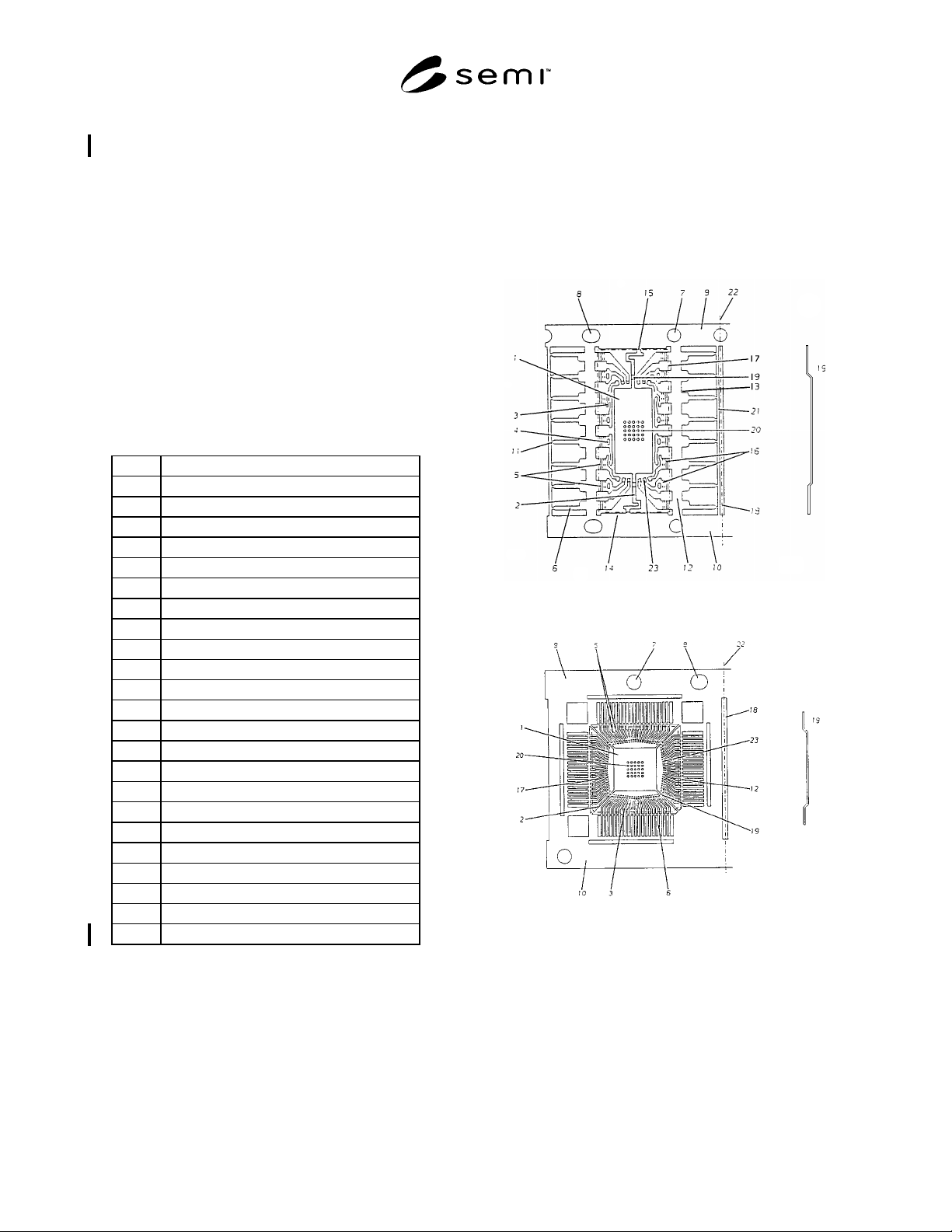
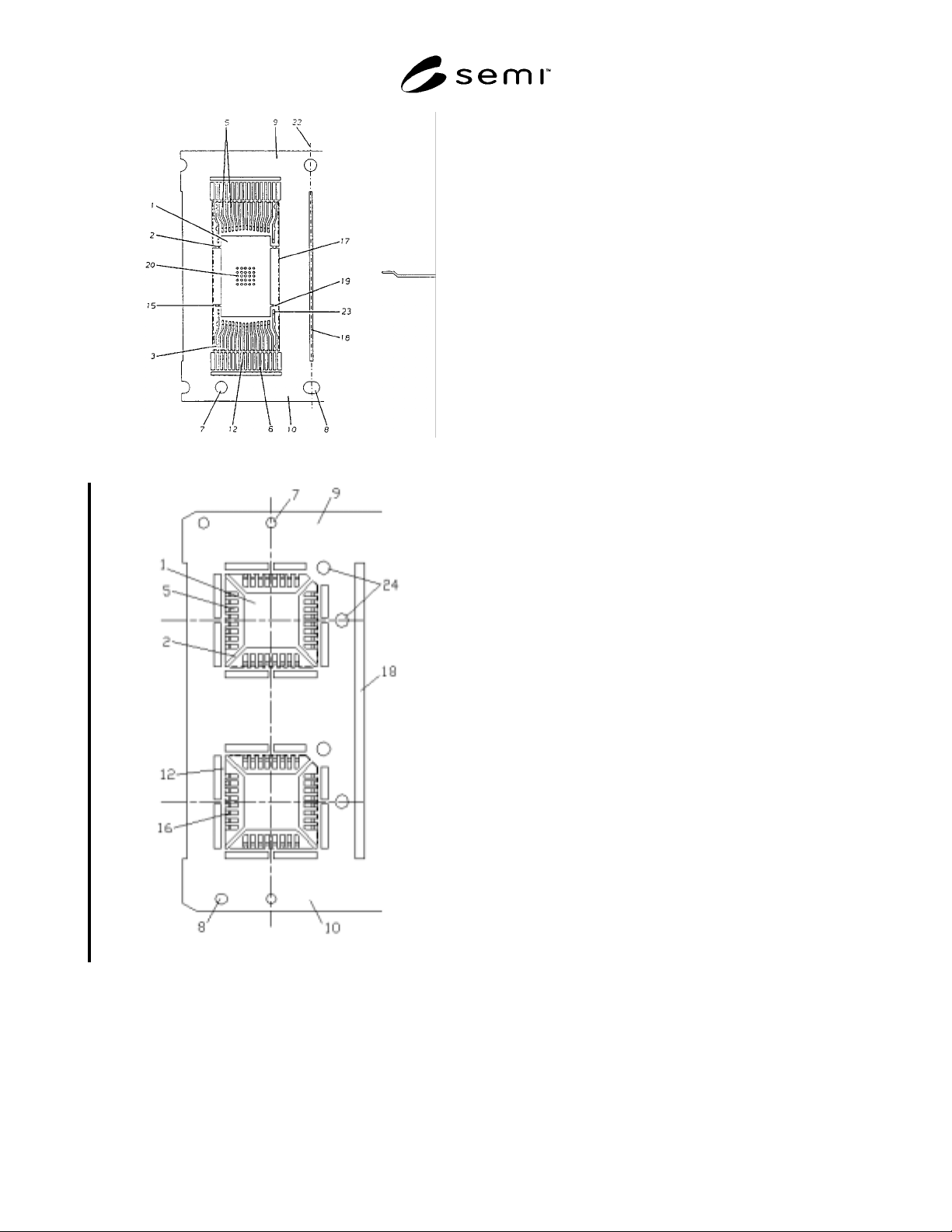
Table 1 Nomenclature for Figures
1 Die Pad
2 Die Pad Support
3 Lead Lock
4 Anchor Hole
5 Inner Lead
6 Outer Lead
7 Standard Pilot Hole
8 Pilot Hole
9 Top Rail Standard Pilot Hole Side
10 Bottom Rail
11 Lead Cut-off Notch
12 Dam Bar
13 Lead Shoulder
14 Mold Dam
15 Bumper Support Cut-off Notch
16 Lead Lock Groove
17 Mold Line
18 Expansion Slot
19 Down Set
20 Die Pad Dimple
21 Side Rail
22 Strip Cut-off Line
23 Coined Area
24 Degate Hole
Figure 1
Figure 2
SEMI G57-0302 © SEMI 1993, 2002 2
Figure 3
Figure 4
NOTICE: These standards do not purport to address
safety issues, if any, associated with their use. It is the
responsibility of the user of these standards to establish
appropriate safety and health practices and determine
the applicability of regulatory limitations prior to use.
SEMI makes no warranties or representations as to the
suitability of the standards set forth herein for any
particular application. The determination of the
suitability of the standard is solely the responsibility of
the user. Users are cautioned to refer to manufacturer’s
instructions, product labels, product data sheets, and
other relevant literature respecting any materials
mentioned herein. These standards are subject to
change without notice.
The user’s attention is called to the possibility that
compliance with this standard may require use of
copyrighted material or of an invention covered by
patent rights. By publication of this standard, SEMI
takes no position respecting the validity of any patent
rights or copyrights asserted in connection with any
item mentioned in this standard. Users of this standard
are expressly advised that determination of any such
patent rights or copyrights, and the risk of infringement
of such rights, are entirely their responsibility.
Copyright by SEMI® (Semiconductor Equipment and Materials
International), 3081 Zanker Road, San Jose, CA 95134. Reproduction o
f
the contents in whole or in part is forbidden without express writte
n
consent of SEMI.
SEMI G58-94 © SEMI 19941
SEMI G58-94
SPECIFICATION FOR CERQUAD PACKAGE CONSTRUCTIONS
1 Preface
1.1 Purpose — This specification defines the
acceptance criteria for Cerquad package components
and includes requirements for the base, leadframe,
window frame, cap and sealing glass materials.
1.2 Scope — This specification applies to all Cerquad
packages which have a leadframe sandwich between
two ceramic pieces — the base and the window frame
— and sealed by glass, and a cap with a similar glass
seal.
NOTE 1: The base, leadframe and window frame may be
purchased as separate components or as a completed
assembly.
1.3 Units — U.S. Customary (inch -pound) or metric
(SI) units may be used at the customer’s discretion.
This specification uses U.S. Customary units as the
prime unit.
NOTE 2: In the figures only U.S. Customary units are shown.
2 Applicable Documents
2.1 Order of Precedence — To avoid conflicts, the
order of precedence when ordering package
components shall be as follows:
Purchase Order
Customer’s Component Drawings
This Specification
Referenced Documents
2.2 Referenced Documents
2.2.1 SEMI Specifications
SEMI G21 — Plating Integrated Circuit Leadframes
SEMI G23 — Measuring the Inductance of Package
Leads
SEMI G24 — Measuring the Lead-to-Lead and Loading
Capacitance of Package Leads
SEMI G25 — Measuring the Resistance of Package
Leads
Compilation of Terms
2.2.2 JEDEC Specifications
1
Pub. No. 95 — Registered and Standard Outlines for
Semiconductor Devices
1 JEDEC, 2001 Eye Street N.W., Washington, DC 20006.
2.2.3 Military and Federal Specifications
2
MIL-STD-105 — Sampling Procedures and Tables for
Inspection by Attributes
MIL-STD-883 — Test Methods and Procedures for
Microelectronics
MIL-STD-1835 — Microcircuit Case Outlines
MIL-G-45204 — Gold Plating — Electrodeposited
MIL-M-38510 — General Specification for
Microcircuits
3 Selected Definitions
3.1 blister (bubble) metallization — an enclosed
locallized separation of the metallization from its base
material (such as ceramic or another metallization layer
component) that does not expose the underlying layer.
3.2 burr — an adherent fragment of parent material at
a component edge. In leadframes, the metal burr, due to
the stamping operation, may be in the horizontal or
vertical direction to the surface. In ceramic packages,
this type of characteristic is called a fin.
3.3 camber (ceramic) — arching o f a nominally flat
ceramic body.
3.4 chip — region of material missing from a
component (e.g., ceramic from a package, or solder
from a preform). The region does not progress
completely through the component and is formed after
the component is manufactured. Chip size is defined by
its length, width and depth from a projection of the
design planform. Also called chipout. (See Figure 1.)
3.5 crack — a cleavage or fracture that extends to the
surface of a semiconductor package or solder preform.
The crack may or may not pass through the entire
thickness of the package or preform.
3.6 critical seal area — on a semiconductor package,
the area bounded by the shortest nominal design
distance from the largest cavity, usually the wire bond
cavity, to the edge of the package or ceramic layer
forming the seal area. (See Figure 2.)
3.7 fin — on a ceramic package or cap, a fine
feathery-edged projection of parent ceramic material on
the corner of the ceramic body.
2 Military Standards, Naval Publications and Form Center, 5801
Tabor Avenue, Philadelphia, PA 19120