semi合集-English.pdf - 第4005页
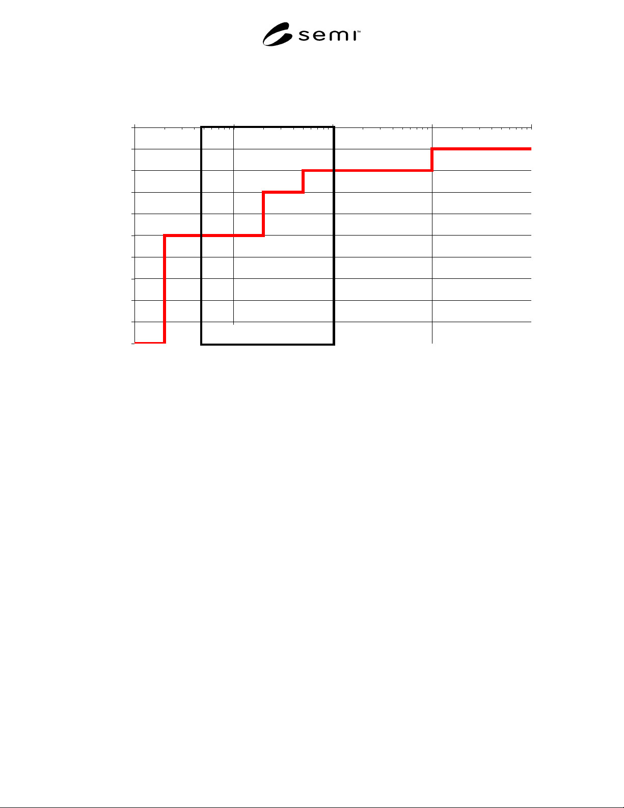
SEMI F47-0200 © SEMI 199 9, 2000 6 0 10 20 30 40 50 60 70 80 90 100 0.01 0.1 1 10 100 Duration of Voltage S ag in Seconds Perce nt of Equipment Nominal Voltage Area included in Specifi cation 0.05 to 1 second 0.02 Figure…

SEMI F47-0200 © SEMI 1999, 20005
RELATED INFORMATION 1
RELATIONSHIP TO OTHER ELECTRICAL STANDARDS
NOTE: This related information is not an official part of
SEMI F47 and is not intended to modify or supersede the
official standard. It has been derived from the work of the
originating task force. Determination of the suitability of
the material is solely the responsibility of the user.
R1-1 Basis for this Industry-Specific
Semiconductor Standard
R1-1.1 The Information Technology Industry
Council (ITIC) “CBEMA-curve,” contained in IEEE
446, IEEE 1100, and SEMI E51, was used as a
starting point in establishing recommended ride-
through limits. The following curve (see Figure R1-
1) was developed to define voltage sag ride-through
for use with semiconductor processing equipment.
Primarily due to testing limitations, only the portion
between 0.05 seconds (50 milliseconds) and 1.0
seconds was selected for inclusion in the
specification. As future test equipment, methods, and
data are developed the specified duration limits may
be expanded. Recommended voltage sag ride-
through capability limits from zero to 100 seconds
are included here for reference (see Figure R1-1).
While not currently included in this SEMI
specification the wider range should be considered
when designing equipment and selecting
components.
R1-1.2 Over voltage conditions also covered in the
ITIC CBEMA-curve contained in IEEE 446, IEEE
1100, and SEMI E51, are not considered in the scope
of this industry-specific specification primarily due to
the extremely low number of semiconductor
equipment interruptions caused by over voltage
events. While not in the scope of this specification,
over voltage conditions should not be ignored and
use of existing equipment protection techniques
should be continued (see SEMI E51 or IEEE 446 for
generic equipment over voltage ride-through
specifications).
R1-2 Relationship to Generic Electrical
Standards
R1-2.1 This SEMI standard is intended to be
coordinated with related SEMI, IEC and IEEE
standards. The relationship of this SEMI
specification to many other standards that address
equipment immunity, test methods, and safety was
considered in development of this specification. For
example, the emerging IEC Generic Immunity standard
for industrial environments currently published by
CENELEC as EN 50082-2 recommends a generic
equipment immunity limit for Europe. When published
by IEC, this standard will provide a generic equipment
voltage sag immunity limit. Another example is the US
National Fire Protection Association on Industrial
Machinery (NFPA 79), which sets a generic equipment
voltage sag immunity limit for the United States.
R1-2.2 These emerging generic limits were considered in
the establishment of ride-through limits for semiconductor
equipment. However, most generic equipment limits are
less stringent than the existing CBEMA-curve currently
referenced in SEMI E51. For most installations meeting
the CBEMA limits (a specification which was developed
for computer business equipment) still results in an
unacceptable number of semiconductor equipment
interrupts. Therefore, the requirements in this
international standard were developed to better suit the
semiconductor industry. While more stringent, this
industry-specific specification is not in conflict with
known generic equipment regulations from other regions
or generic equipment standards from other organizations.
R1-2.3 Another published IEC standard defines a generic
immunity test method for voltage sags (dips), IEC 61000-
4-11. This standard does not provide limits but does
provide a voltage sag test method for single-phase
equipment rated less than 16 amps. It has been
considered in defining voltage sag ride-through
parameters and it may provide an interim voltage sag
immunity test method. As noted in this document, a test
method for three-phase equipment greater than 16 amps is
being developed for use with semiconductor equipment.
R1-2.4 The generic type standards developed for
industrial or consumer equipment by organizations like
IEC, ITIC, and IEEE provide a foundation for industry-
specific standards like those published by SEMI
Standards. In acknowledgement of this tiered approach to
standardization there are provisions for recognizing
industry-specific or product-type standards by
organizations like IEC. Typically, product-type standards
when developed by industry-specific organizations take
precedent over the broader based generic industrial
standards.
SEMI F47-0200 © SEMI 1999, 2000 6
0
10
20
30
40
50
60
70
80
90
100
0.01 0.1 1 10 100
Duration of Voltage Sag in Seconds
Percent of Equipment Nominal Voltage
Area included in Specification
0.05 to 1 second
0.02
Figure R1-1
Recommended Semiconductor Equipment Voltage Sag Ride-Through Capability Curve
from 0 to 100 Seconds
NOTICE: SEMI makes no warranties or
representations as to the suitability of the standards set
forth herein for any particular application. The
determination of the suitability of the standard is solely
the responsibility of the user. Users are cautioned to
refer to manufacturer’s instructions, product labels,
product data sheets, and other relevant literature
respecting any materials mentioned herein. These
standards are subject to change without notice.
The user’s attention is called to the possibility that
compliance with this standard may require use of
copyrighted material or of an invention covered by
patent rights. By publication of this standard, SEMI
takes no position respecting the validity of any patent
rights or copyrights asserted in connection with any
item mentioned in this standard. Users of this standard
are expressly advised that determination of any such
patent rights or copyrights, and the risk of infringement
of such rights, are entirely their own responsibility.
Copyright by SEMI® (Semiconductor Equipment and Materials
International), 3081 Zanker Road, San Jose, CA 95134. Reproduction o
f
the contents in whole or in part is forbidden without express written
consent of SEMI.
SEMI F48-0600 © SEMI 20001
SEMI F48-0600
TEST METHOD FOR DETERMINING TRACE METALS IN POLYMER
MATERIALS
This test method was technically approved by the Global Facilities Committee and is the direct responsibility
of the North American Facilities Committee. Current edition approved by the North American Regional
Standards Committee on March 2, 2000. Initially available on www.semi.org April 2000; to be published
June 2000.
1 Purpose
1.1 This method provides a procedure for determining
the nonvolatile trace inorganic impurities in bulk
polymeric materials.
2 Scope
2.1 Following digestion by dry ashing (DDA) or
digestion in closed vessel (DCV) preparation
techniques, samples previously obtained and cleaned
according to SEMI F40 are analyzed for trace
inorganics using inductively coupled plasma-mass
spectrometry (ICP–MS), graphite furnace atomic
absorption spectroscopy (GFAAS), and/or inductively
coupled plasma-atomic emission spectroscopy (ICP–
AES).
2.2 Materials for analysis include, but are not limited
to:
• Raw polymer materials (resins), such as pellets of
perfluoroalkoxy (PFA), polyvinylidene fluoride
(PVDF), ethylenechlorotrifluoroethylene (ECTFE),
polyetheretherketone (PEEK), polypropylene (PP),
polyethylene (PE), acetal resin, polyvinyl chloride
(PVC), Perfluoromethylether-based Perfluoro-
alkoxy (MFA) and powders of polytetrafluoro-
ethylene (PTFE).
• Polymer components of tubing, piping, fittings,
valves, regulators, filter housings, filter cartridges,
O–rings and gaskets used in ultrapure water (UPW)
and liquid chemical distribution systems (LCDS).
See Section 3.8 for further information.
• Ion-exchange resins
• Polymer products used in the manufacturing of
semiconductor devices, such as wafer carriers and
wands, as well as accessories internal to wet
equipment (e.g., drums in spin rinse dryers, tanks
in quick dump rinsers). See Section 3.8 for further
information.
2.3 The DDA sections of this document refer to an
ashing technique, whereby the sample is placed into a
platinum or quartz crucible and thermally decomposed.
Thermal decomposition in muffle furnace or microwave
muffle furnace may also be used. Additionally, oxygen
plasma may be used separately or in conjunction with
these techniques.
2.4 The DCV sections of this document refer to closed
vessel microwave acid decomposition at elevated
temperature and pressure. Alternatively closed vessel
thermal conduction heating may also be applied.
2.5 ICP–MS, GFAAS, and ICP–AES are all
appropriate methods for inorganic analysis. ICP–MS is
the preferred method because it is more sensitive and
efficient. Alternate procedures may be used if they
meet the same analytical performance criteria. Each
laboratory is responsible for verifying the validity of
each method within its own operation.
2.6 This method is applicable for the elements found
in Table 1:
Table 1 List of Applicable Elements (See NOTE 1.)
Aluminum Magnesium
Barium Manganese
Calcium Nickel
Chromium Potassium
Cobalt Sodium
Copper Strontium
Iron Tin
Lead Titanium
Lithium Zinc
Molybdenum Zirconium
NOTE 1: See Limitations, Section 3.3.
2.7 This method may be used for other materials, or
other nonvolatile elements, if the end-user wishes and
performance is demonstrated for the analyte of interest,
in the matrices of interest, at the concentration levels of
interest.
2.8 This standard does not purport to address safety
issues, if any, associated with its use. It is the
responsibility of the users of this standard to establish
appropriate safety and health practices and determine
the applicability of regulatory limitations prior to use.
3 Limitations
3.1 The accuracy of the method is limited by the
detection limits of the instruments and by the sample
preparation procedure.