semi合集-English.pdf - 第7436页
5 Terminology 5.1 Acro nyms related to wafer flatness param eters as defined in SEMI M 1 , Appendi x 1, Flatness Decision Tree, are summarized in Table 1. NOTE 1: The most comm only specified flatnes s measure- ments for…

SEMI MF1530-1104
TEST METHOD FOR MEASURING FLATNESS, THICKNESS, AND
TOTAL THICKNESS VARIATION ON SILICON WAFERS BY
AUTOMATED NON-CONTACT SCANNING
This test method was technically approved by the Global Silicon Wafer Committee and is the direct
responsibility of the North American Silicon Wafer Committee. Current edition approved for publication by
the North American Regional Standards Committee on July 11, 2004. Initially available at www.semi.org
September 2004; to be published November 2004. Original edition published by ASTM International as
ASTM F 1530-94. Last previous edition SEMI MF1530-0704.
1 Purpose
1.1 Flatness, thickness and thickness variation are vital
factors affecting the yield of semiconductor device
processing.
1.2 Knowledge of these characteristics can help the
producer and consumer determine if the dimensional
characteristics of a specimen wafer satisfy given
geometrical requirements.
1.3 This test method is suitable for measuring the
flatness and thickness of wafers used in semiconductor
device processing in the as-sliced, lapped, etched,
polished, epitaxial or other layer condition.
2 Scope
2.1 This test method covers a noncontacting,
nondestructive procedure to determine the thickness
and flatness of clean, dry, semiconductor wafers in such
a way that no physical reference is required.
2.2 This test method is applicable to wafers 50 mm or
larger in diameter, and 100 m (0.004 in.)
approximately and larger in thickness, independent of
thickness variation and surface finish, and of wafer
shape.
2.3 This test method measures the flatness of the front
wafer surface as it would appear relative to a specified
reference plane when the back surface of the water is
ideally flat, as when pulled down onto an ideally clean,
flat chuck. It does not measure the free-form shape of
the wafer.
2.4 Because no chuck is used as a measurement
reference, this test method is relatively insensitive to
microscopic particles on the back surface of the wafer.
2.5 The values stated in SI units are to be regarded as
the standard. The values given in parentheses are for
information only.
NOTICE: This standard does not purport to address
safety issues, if any, associated with its use. It is the
responsibility of the user of this standard to establish
appropriate safety and health practices and determine
the applicability of regulatory or other limitations prior
to use.
3 Limitations
3.1 Any relative motion between the probes and along
the probe measuring axis during scanning produces
error in the lateral position equivalent-measurement
data.
3.2 Most equipment systems capable of this
measurement have a definite range of wafer thickness
combined with sori/warp (dynamic range) that can be
accommodated without readjustment. If the sample
moves outside this dynamic range during either
calibration or measurement, results may be in error. An
overrange signal can be used to alert the operator and
measurement data examiners to this event.
3.3 The quantity of data points and their spacing may
affect the measurement results (see Section 7.1.5.2).
3.4 Site flatness measurements may be affected if the
site boundaries and corners do not contain data array
elements. This effect may be reduced through
interpolation techniques.
4 Referenced Standards
4.1 SEMI Standards
SEMI M1 — Specifications for Polished
Monocrystalline Silicon Wafers
SEMI M20 — Practice for Establishing a Wafer
Coordinate System
SEMI MF1241 — Terminology of Silicon Technology
4.2 ASTM Standard
1
E 691 — Practice for Conducting an Interlaboratory
Study to Determine the Precision of a Test Method
NOTICE: Unless otherwise indicated, all documents
cited shall be the latest published versions.
1 Available from ASTM International, 100 Barr Harbor Drive, West
Conshohocken, PA 19428, Tel: 610-832-9500, Fax: 610-832-9555,
Website
http://www.astm.org. Appears in Volume 14.02 of Annual
Book of ASTM Standards.
SEMI MF1530-1104 © SEMI 2003, 2004 1
5 Terminology
5.1 Acronyms related to wafer flatness parameters as
defined in SEMI M1, Appendix 1, Flatness Decision
Tree, are summarized in Table 1.
NOTE 1: The most commonly specified flatness measure-
ments for advanced IC production in 2004, the time of the last
revision of this standard, are SFQR with a site size of either
26 mm by 8 mm or 25 mm by 8 mm and GBIR (TTV).
5.2 Definitions related to wafer flatness can be found
in SEMI M1.
5.3 Definitions of other terms related to silicon
material technology can be found in SEMI MF1241.
6 Summary of Test Method
6.1 A calibration procedure is performed. This sets the
instrument's scale factor and other constants.
6.2 The wafer is supported by a small-area chuck and
is scanned along a prescribed pattern by both members
of an opposed pair of probes.
6.3 The paired displacement values are used to
construct a thickness data array (t[x,y]). This array
represents the front surface of the wafer when the back
surface of the wafer is ideally flat, as when pulled down
onto and ideally clean, flat chuck.
6.4 The data array is used to produce one or more of
the parameters required by the application.
6.4.1 If flatness measurements are required, a reference
plane and a focal plane suitable to the application are
constructed on the back or front surface.
6.5 Thickness or flatness, or both, values are calculated
and reported, as required.
7 Apparatus
7.1 Measuring Equipment — consisting of wafer-
holding device, multiple-axis transport mechanism,
probe assembly with indicator, and system controller/
computer, including data processor and suitable
software.
7.1.1 The measuring equipment shall have means to
input the choices listed in the Procedure (see Section 12
).
7.1.2 The measuring equipment shall be direct reading
with all necessary calculations performed internally and
automatically as outlined in Section 13 .
7.1.3 The system shall be equipped with an overrange
signal.
7.1.4 Instrument data reporting resolution shall be 10
nm or smaller.
7.1.5 The measuring equipment contains the following
subsystems:
7.1.5.1 Wafer-holding device, for example a chuck
whose face is perpendicular to the measurement axis,
and on which the wafer is placed for the measurement
scan. The nature and size of the wafer holding device
shall be agreed upon between the parties to the test.
7.1.5.2 Multiple-axis transport mechanism, which
provides a means for moving the wafer-holding device,
or the probe assembly, perpendicularly to the
measurement axis in a controlled fashion in several
directions. This motion must permit data gathering
over a prescribed scan pattern within the entire fixed
quality area. Data point spacing to be used shall be
agreed upon between the parties to the test.
7.1.5.3 Probe assembly with paired noncontacting
displacement-sensing probes, probe supports, and
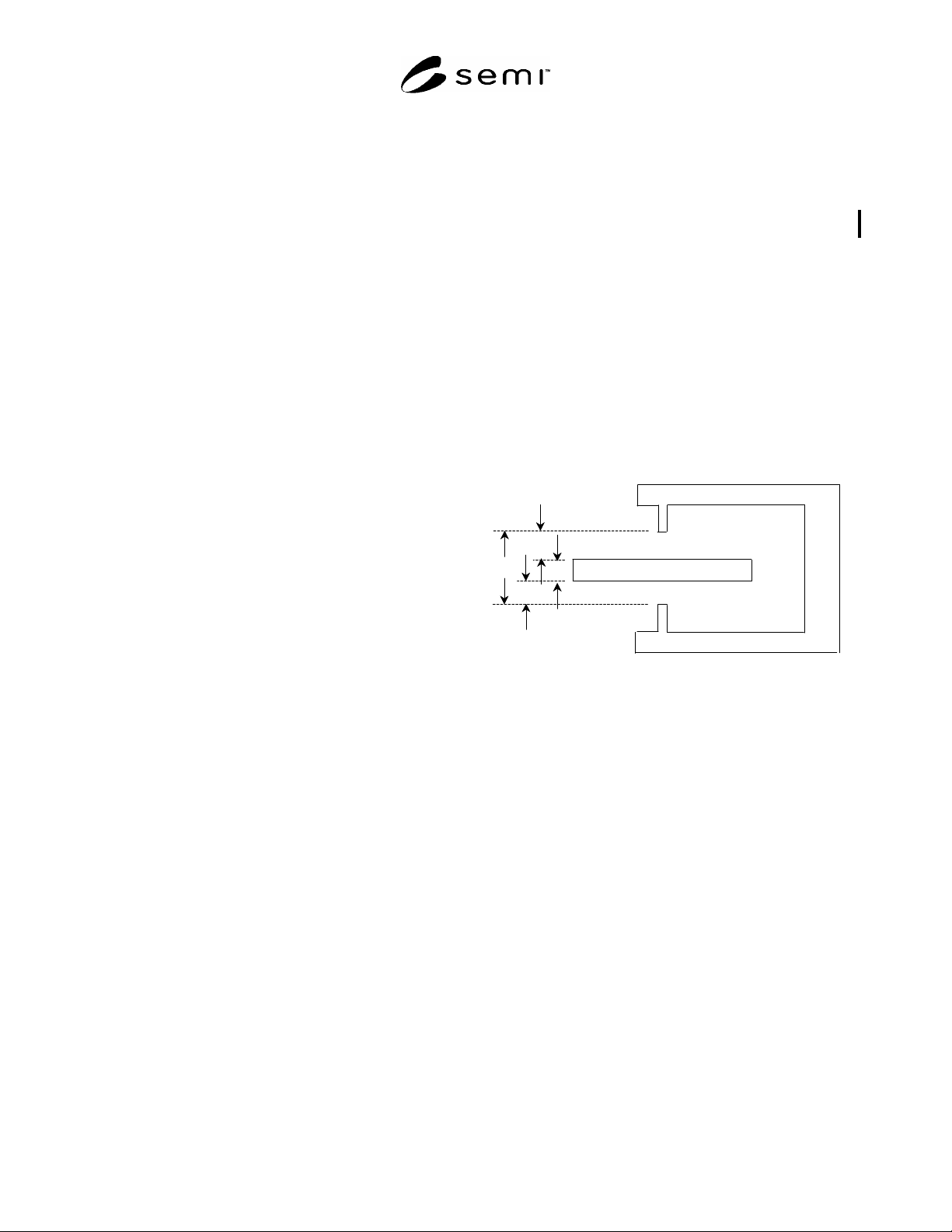
indicator unit (see Figure 1).
t
a
b
D
Probe A
Probe B
Wafer
Fixture
t
a
b
D
Probe A
Probe B
Wafer
Fixture
Figure 1
Schematic View of Wafer, Probes, and Fixture
7.1.5.3.1 The probes shall be capable of independent
measurement of the distances a and b between the
probed site on each surface of the sample wafer and the
nearest probe surface.
7.1.5.3.2 The probes shall be mounted above and
below the wafer in a manner so that the probed site on
one surface of the wafer is opposite the probed site on
the other.
7.1.5.3.3 The common axis of these probes is the
measurement axis.
7.1.5.3.4 The probe separation D shall be kept constant
during calibration and measurement.
7.1.5.3.5 Displacement resolution shall be 10 nm or
better.
7.1.5.3.6 The probe sensor size shall be 4 × 4 mm, or
other value to be agreed upon between the parties to the
test.
SEMI MF1530-1104 © SEMI 2003, 2004 2
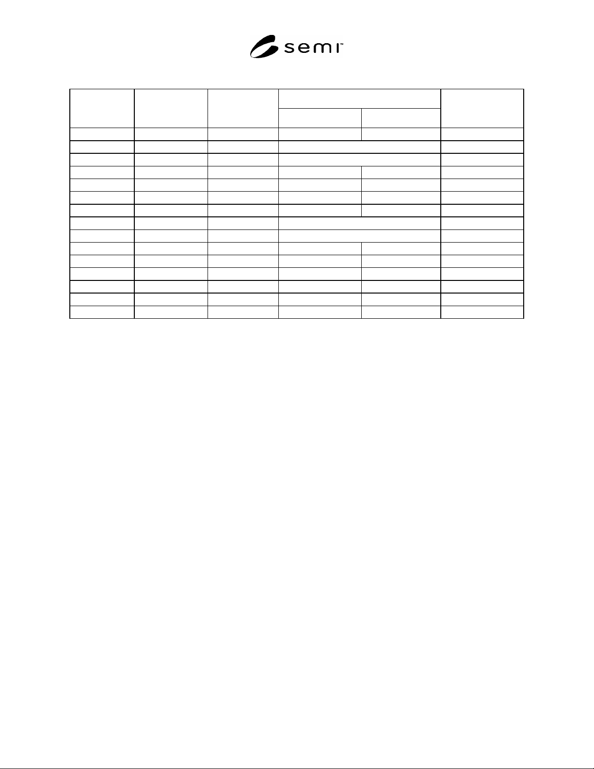
Table 1 Acronyms for Wafer Flatness Parameters
Reference Plane
Acronym
Measurement
Method
Reference Surface
Construction Area
Measurement
Parameter
GBIR Global Back Ideal back surface Entire FQA Range (TIR)
GF3R Global Front Three-point Range (TIR)
GF3D Global Front Three-point Deviation (FPD)
GFLR Global Front Least squares Entire FQA Range (TIR)
GFLD Global Front Least squares Entire FQA Deviation (FPD)
SBIR Site Back Ideal back surface Entire FQA Range (TIR)
SBID Site Back Ideal back surface Entire FQA Deviation (FPD)
SF3R Site Front Three-point Range (TIR)
SF3D Site Front Three-point Deviation (FPD)
SFLR Site Front Least squares Entire FQA Range (TIR)
SFLD Site Front Least squares Entire FQA Deviation (FPD)
SFQR Site Front Least squares Site Range (TIR)
SFQD Site Front Least squares Site Deviation (FPD)
SFSR Site Front Least squares Sub-site Range (TIR)
SFSD Site Front Least squares Sub-site Deviation (FPD)
8 Materials
8.1 Set-up Masters — suitable to accomplish
calibration and standardization as recommended by the
equipment manufacturer.
8.2 Reference Wafer — with total thickness variation
(TTV) value and flatness value similar to the product or
process to be monitored and with a data set that is used
to determine the level of agreement between the data
set obtained by the measuring equipment under test and
the reference wafer data set (see Section 9 ).
9 Suitability of Measuring Equipment
9.1 Determine the suitability of the measuring
equipment with the use of a reference wafer and its
associated data set in accordance with the procedures of
Sub-section 9.2 , or by performance of a statistically-
based instrument repeatability study to ascertain
whether the equipment is operating within the
manufacturer's stated specification for repeatability.
9.1.1 The reference wafer data set is a set of thickness
or flatness parameters based on corrected data in that all
possible interferences have been removed and the data
has been replanarized in accordance with this method.
9.1.2 Each reference wafer (artifact) is accompanied by
its own data set, the reference data set (RDS), in which
each parameter value is the average of a number of
values obtained for that parameter over a number of
“passes” (repeat measurements). The artifact is
measured on a measurement equipment under test and
its RDS is compared against the resultant-measured
sample data set. Delta-parameter and other values are
computed from the differences. The parameter used to
determine agreement between the artifact and the
measuring equipment under test and the acceptable
level of this agreement is to be agreed upon between the
parties to the test.
9.2 Procedure
9.2.1 Select a reference wafer of appropriate criteria
together with its associated reference data set (RDS).
9.2.2 Measure the reference wafer on the measurement
equipment under test to obtain a sample data set (SDS).
9.2.3 Subtract the two data sets on a parameter basis to
obtain a difference data set (DDS):
DDSSDSRDS
(1)
9.2.3.1 The DDS represents the differences between
the measurements made on the measuring equipment
under test and the reference data set. The DDS contains
many values.
9.2.4 The simplest metric that can be used to determine
acceptability is maximum difference, the largest
absolute value in the DDS. This represents the worst-
case disagreement between the results obtained from
the measurement equipment under test and the
reference data. Accept the measurement equipment as
suitable for measurement if the maximum difference is
less than a value that is agreed upon between the parties
to the test.
SEMI MF1530-1104 © SEMI 2003, 2004 3