semi合集-English.pdf - 第1036页
SEMI E141-0705 © SEMI 2005 9 NOTE: T he P C S A configuration is shown for a single-wavelength ellipsometer. For other configurations, see ¶6.4.1. Figure 1 Schematic of an Ellipsometer System Layer 1: N 1 : n 1 , k 1 Lay…
SEMI E141-0705 © SEMI 2005 8
NOTE 6: The reference samples are typically certified thickness standards using reference materials. For thickness
measurements typical samples are thermal oxides on silicon ranging from 4 nm to 800 nm. For refractive index measurements,
the reference sample thickness is typically in the range from 80 nm to 500 nm.
NOTE 7: SEMI MF576-01 was originally published by ASTM International as ASTM F 576-78. It was formally approved by
ASTM balloting procedures and adhered to ASTM patent requirements. Though ownership of this standard has been transferred
to SEMI, it has not been formally approved by SEMI balloting procedures and does not adhere either to SEMI Regulations
dealing with patents or to SEMI Editorial Guidelines. It was available at www.semi.org, last published by ASTM International as
ASTM F 576-01. Hence in SEMI MF576-01, the notation for parameters required in data acquisition and modeling is aligned but
could not retroactively be fully harmonized with the definitions specified in the presented guide. This does not constitute any
constraints since these few parameters may easily be superseded by the newer definitions provided.
7.7.2 Whenever the thickness and refractive index measurement (if performed) is within specified limits for the
reference sample, the ellipsometer is defined as qualified and hence capable of measuring the respective type of
sample.
7.7.3 The qualification status of an ellipsometer is defined and must be specified by providing the following
parameters: (1) the relevant parameters for sample identification, (2) the relevant optical parameters of the sample,
(3) the expected measurement result, (4) the actual measurement result, (5) the tolerated deviation between the
actual and the expected measurement result, (6) all relevant parameters of the ellipsometer system (e.g. all relevant
parameters of the positions of the optical components) the angle of incidence, and (7) all relevant environmental
parameters.
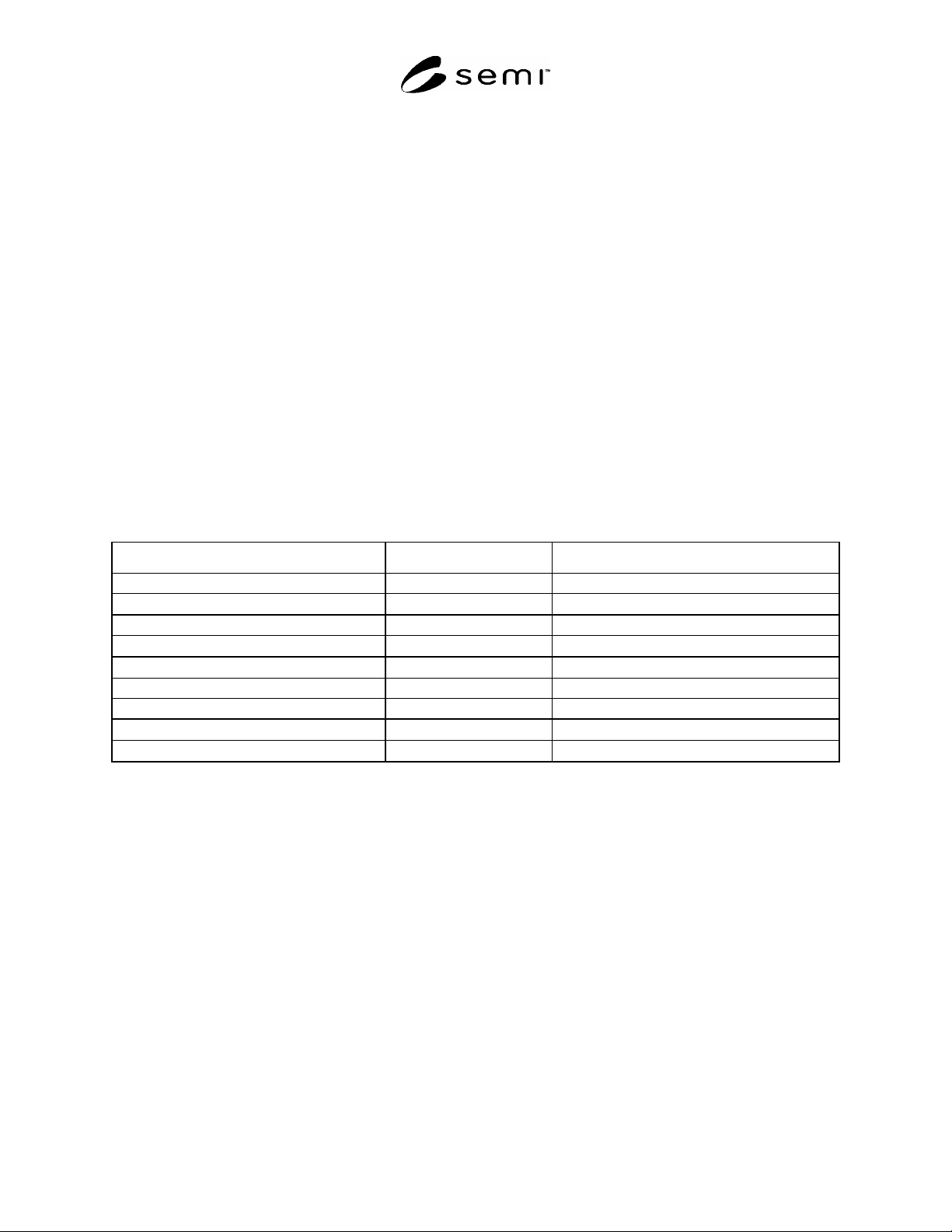
7.7.4 Recommended Units and Symbols — The units as listed in Table 1 are recommended for the description of the
listed parameter.
Table 1 Recommended Units
Physical Quantity Symbol Unit(s)
Metric thickness t µm, nm, Å
Wavelength
µm, nm, Å
Photon energy E eV
Wave number
cm
-1
Angles
,
,
0
,
p
,
c
,
PEM
,
A
° or deg (360° are a full circle)
Electric field vectors E
ip
, E
is
, E
rp
, E
rs
V/m
Optical parameters (refractive indices) N, n, k
no unit
Complex dielectric function
no unit
Pseudo <
>
no unit
#1
See SEMI E30.5 for the preferred thickness unit (Å).
#2
The pseudo dielectric constant <> is calculated from the raw data set using a sample model consisting of only the ambient and substrate
without layers.
SEMI E141-0705 © SEMI 2005 9
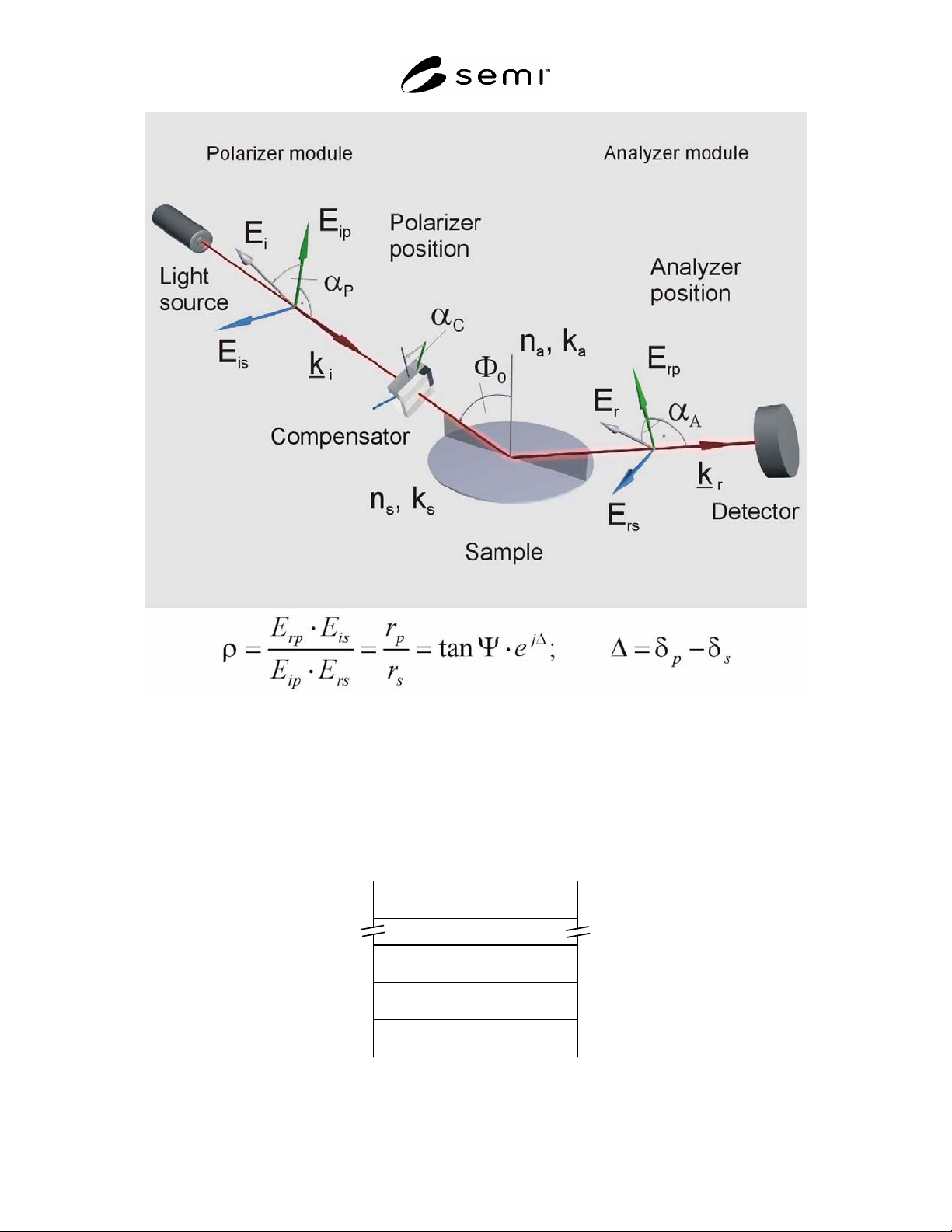
NOTE: The P C S A configuration is shown for a single-wavelength ellipsometer. For other configurations, see
¶6.4.1.
Figure 1
Schematic of an Ellipsometer System
Layer 1: N
1
: n
1
, k
1
Layer 2: N
2
: n
2
, k
2
Substrate medium: N
s
: n
s
, k
s
Layer i: N
i
: n
i
, k
i
Ambient medium: N
a
: n
a
, k
a
Figure 2
Illustration of the Layer Counting Principle

SEMI E141-0705 © SEMI 2005 10
NOTICE: SEMI makes no warranties or representations as to the suitability of the standards set forth herein for any
particular application. The determination of the suitability of the standard is solely the responsibility of the user.
Users are cautioned to refer to manufacturer's instructions, product labels, product data sheets, and other relevant
literature, respecting any materials or equipment mentioned herein. These standards are subject to change without
notice.
By publication of this standard, Semiconductor Equipment and Materials International (SEMI) takes no position
respecting the validity of any patent rights or copyrights asserted in connection with any items mentioned in this
standard. Users of this standard are expressly advised that determination of any such patent rights or copyrights, and
the risk of infringement of such rights are entirely their own responsibility.
Copyright by SEMI® (Semiconductor Equipment and Materials
International), 3081 Zanker Road, San Jose, CA 95134. Reproduction of
the contents in whole or in part is forbidden without express written
consent of SEMI.