semi合集-English.pdf - 第7288页
SEMI MF847-0705 © SEMI 2003, 2005 8 15.2.4 Camera Mountin g Fixture — For clamping the cam era to the mounting track so that th e collimator is aligned with the X-ray beam and the horizontal reference line established by…
SEMI MF847-0705 © SEMI 2003, 2005 7
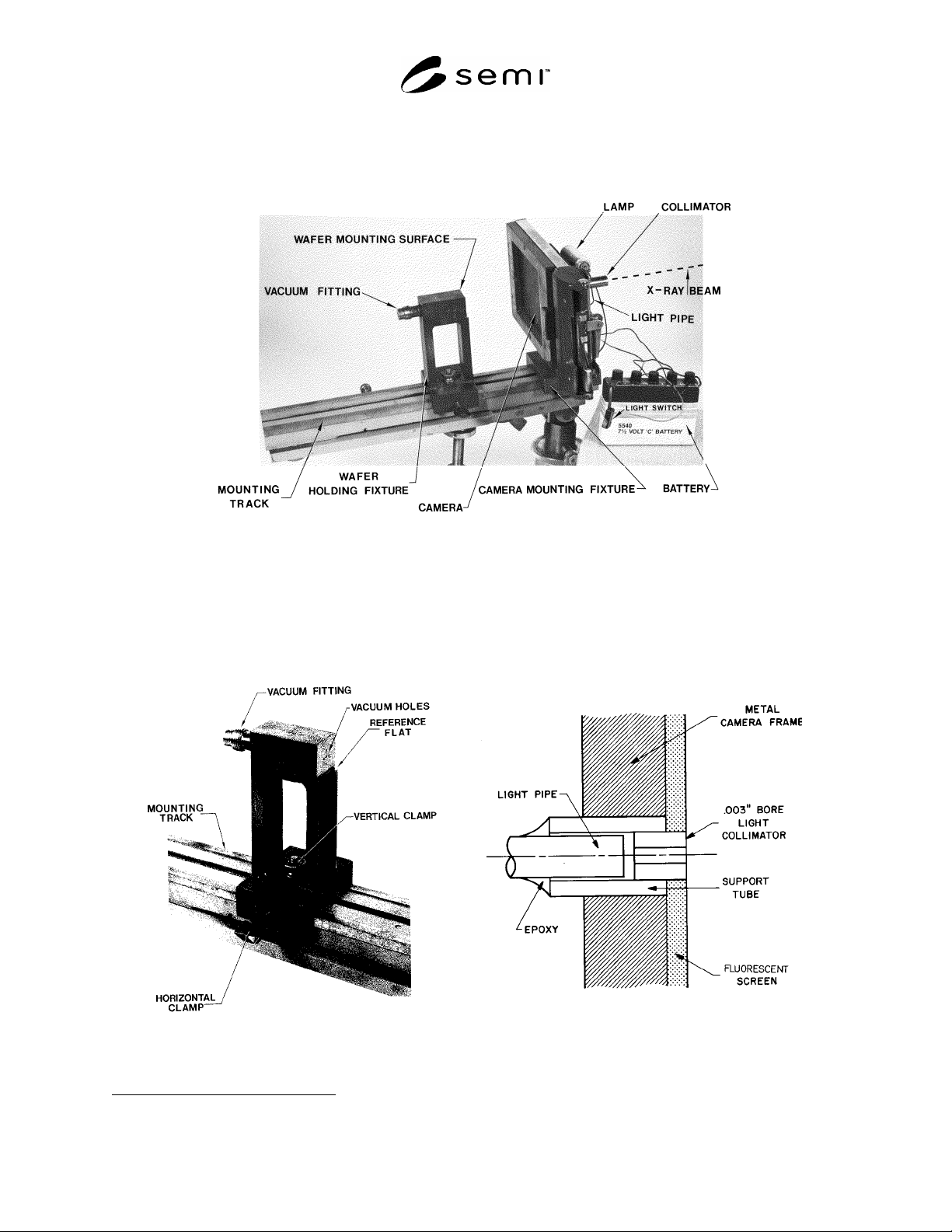
15.2.3 Camera — having a film holder with provision for establishing precisely a horizontal reference line. This is
conveniently done by installing a light source with two light pipes and 75 m (0.003 in.) diameter light collimators
at the midpoint of the shorter dimension of the film, as near to the edges of the sensitive area of the film as possible
(see Figure 5). A tube for collimating the X-ray beam is required at the center of the film holder (see Figure 3).
NOTE: Use of high-speed “instant” film together with a fluorescent screen results in shorter test times than with wet-processed
films.
8
A holder of this type is commercially available. This holder has built into it four reference spots which define two
orthogonal lines which pass through the center of the film when the X-ray beam collimator is located (these reference spots are
not utilized in the present test method). If this type of holder is used, the collimator tube must not protrude above the surface of
the fluorescent screen because of film and clip interference problems during loading and processing of the film.
Figure 3
Photograph of Assembled View of Laue Camera and Wafer Holder
Figure 4
Photograph of Wafer Holding Fixture and
Mounting Track
Figure 5
Section of Laue Camera Platen Showing Light Pipe
and Collimating Tube
8 Schmidt, P. H., and Spencer, E. G., “X-Ray Diffraction Camera Using Polaroid Film,” Rev. Sci. Instrum. 35, 957–958 (1964).
SEMI MF847-0705 © SEMI 2003, 2005 8
15.2.4 Camera Mounting Fixture — For clamping the camera to the mounting track so that the collimator is aligned
with the X-ray beam and the horizontal reference line established by the light-generated dots is parallel with the
upper surface of the mounting track to 1 min of arc (29 m in 100 mm).
15.3 Drafting Head Protractor — With a clear plastic blade and finest vernier divisions of six min of arc or less for
reading the Laue photograph. A straight line, approximately 125 mm (or 5 in.) long, and in line with the centerpoint
of the protractor, is inscribed on the bottom of the plastic blade.
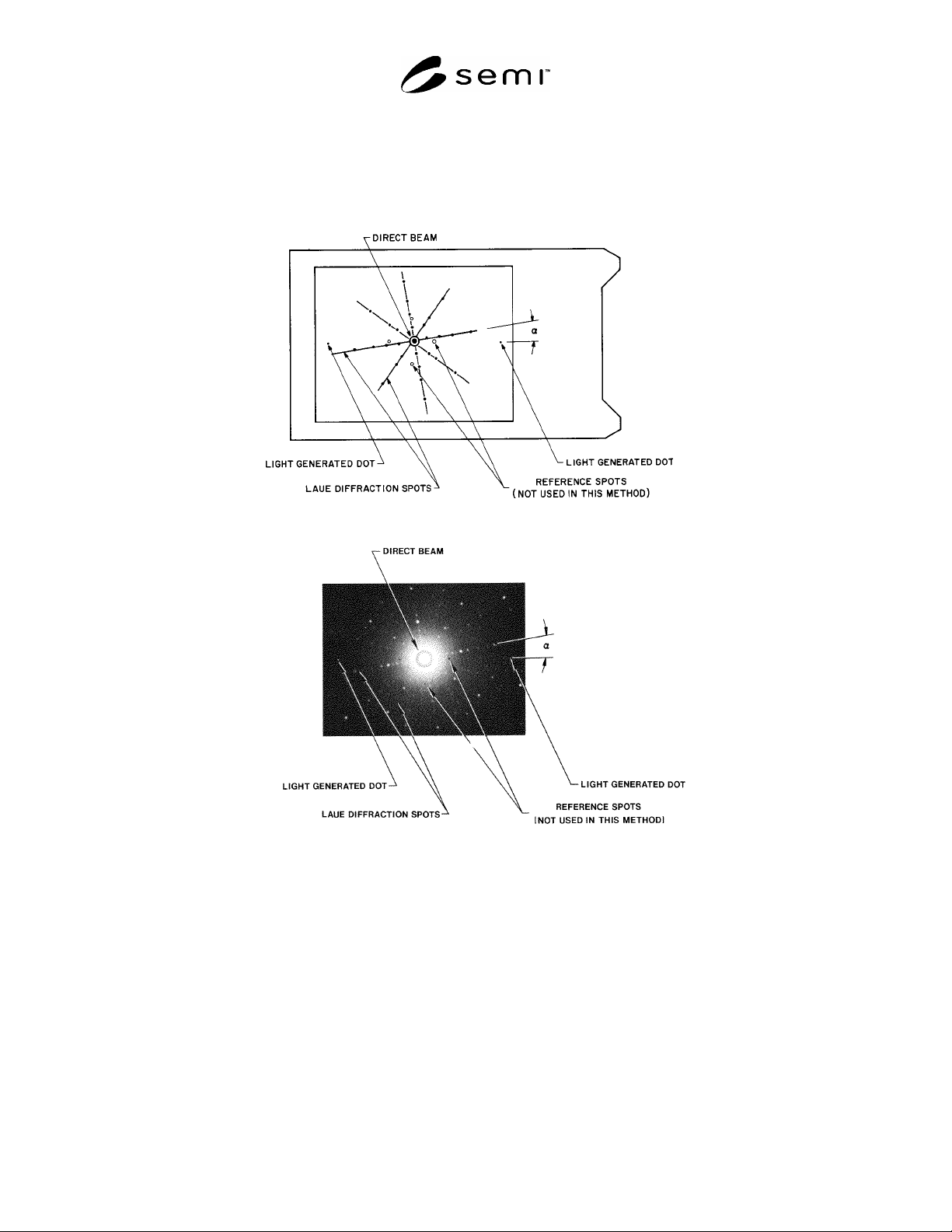
a. Schematic Representation
b. Actual Photograph
Figure 6
Laue Pattern
16 Procedure
16.1 Place the wafer to be tested on the wafer holding fixture so that the flat is resting securely against the reference
flat on the fixture. Turn on the vacuum to hold the wafer securely against the fixture.
16.2 Turn on the X-ray source, adjust the voltage and current (Note 4), and load the film into the camera. Open the
X-ray shutter and expose the film for an appropriate time (Note 5). During exposure, pulse the light to generate the
dots which define the horizontal reference line, and develop the film.
NOTE 4: For a tungsten X-ray tube typical voltage and current are 50 to 60 kV and 20 to 30 mA, respectively.
NOTE 5: Use of high-speed, instant film (ASA 300) and a fluorescent screen results in typical exposure times of 1 to 2 min.
16.3 Read the Laue pattern on the film.

SEMI MF847-0705 © SEMI 2003, 2005 9
16.3.1 Align the scribed line on the underside of the drafting head protractor with the two light-generated dots that
define the horizontal reference line and set the protractor to 0°.
16.3.2 Rotate the protractor so that the scribed line is aligned with the zone of Laue spots that (1) passes through the
center of the pattern and (2) is nearest to the horizontal reference line (see Figure 6).
16.3.3 Read to the nearest 0.1° (6 min) the angle on the protractor and record the value as the angular deviation,
.
17 Report
17.1 Report the following information:
17.1.1 Identity of samples tested including vendor and vendor lot identity,
17.1.2 Date of test and identity of operator making the measurements,
17.1.3 Specified flat and surface orientations,
17.1.4 The measured angular deviation for each wafer, and
17.1.5 The photograph or a copy of the photograph of the Laue pattern for each wafer.
18 Precision and Bias
18.1 The single-instrument, multi-operator precision of this test method was estimated by extensive testing with
three operators. This test yielded a distribution of readings with a 1-s value of 7 min of arc.
19 Keywords
19.1 crystallographic orientation; flats; Laue diffraction; silicon; single crystal
NOTICE: SEMI makes no warranties or representations as to the suitability of the standards set forth herein for any
particular application. The determination of the suitability of the standard is solely the responsibility of the user.
Users are cautioned to refer to manufacturer's instructions, product labels, product data sheets, and other relevant
literature, respecting any materials or equipment mentioned herein. These standards are subject to change without
notice.
By publication of this standard, Semiconductor Equipment and Materials International (SEMI) takes no position
respecting the validity of any patent rights or copyrights asserted in connection with any items mentioned in this
standard. Users of this standard are expressly advised that determination of any such patent rights or copyrights, and
the risk of infringement of such rights are entirely their own responsibility.
Copyright by SEMI® (Semiconductor Equipment and Materials
International), 3081 Zanker Road, San Jose, CA 95134. Reproduction of
the contents in whole or in part is forbidden without express written
consent of SEMI.