semi合集-English.pdf - 第4572页
SEMI D31-1102 © SEMI 2002 5 NOTICE: SEMI makes no warranties or represen tations as to the suitability o f the standards set forth herein for any particular application. The determination of the suitability of the standa…
SEMI D31-1102 © SEMI 2002 4
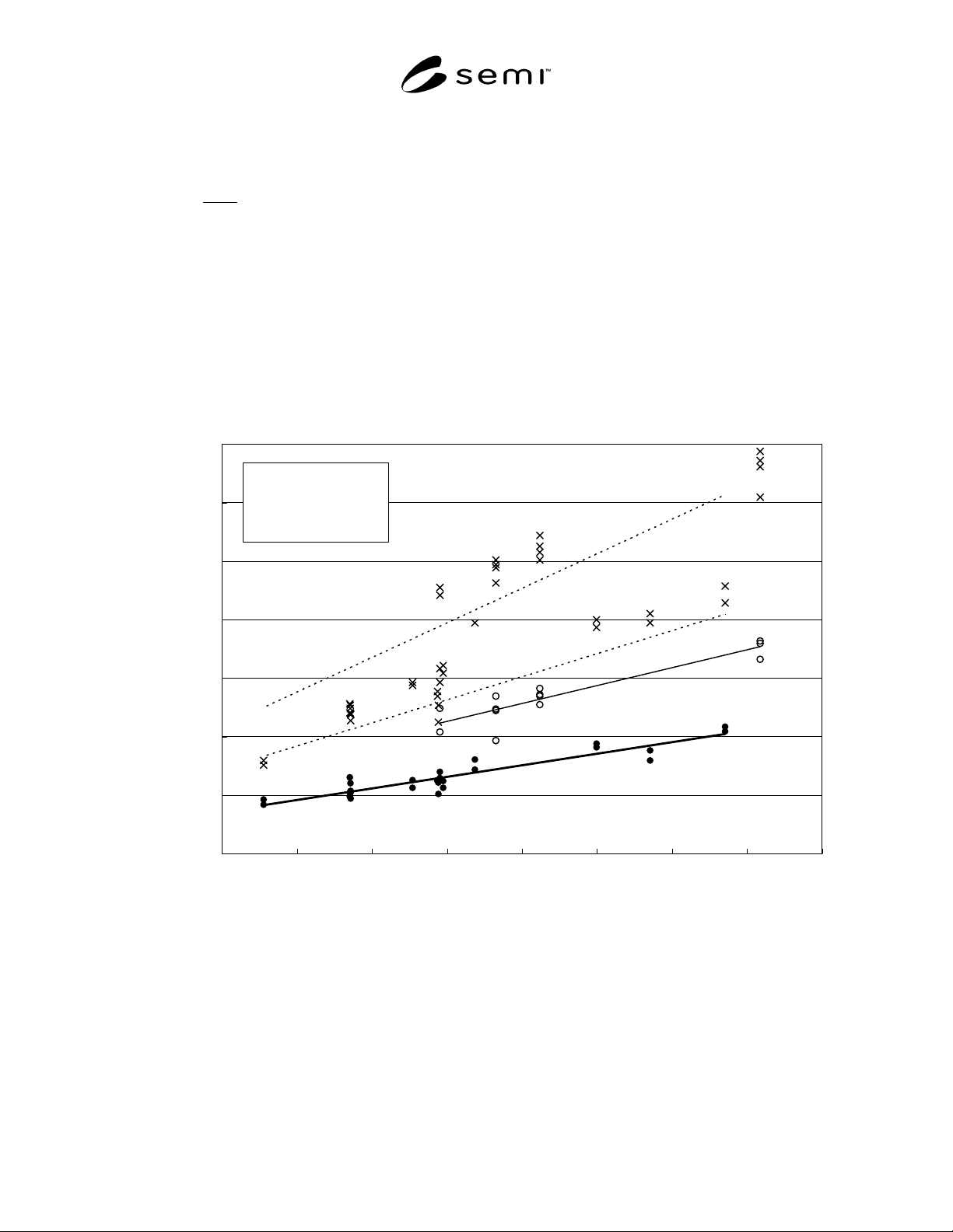
seems to be the boundary. Here we propose Equation 1
which regressively analyzes the ● in Figure 1 as
criteria for standardization.
72.0
1
97.1
33.0
+
=
S
Cjnd
….. Equation 1
R1-3.4 The criteria for standardization, jnd, is
determined by the C jnd straight line, but we also
propose, based on this criteria, quality levels for other
visible muras. Figure 1 shows straight lines made up of
2.0 jnd and 3.0 jnd. × is distinct contrast for the
Expert group, but in cases besides 1-pixel wide muras,
it can be understood to be distributed slightly above the
2.0 jnd straight line.
R1-3.5 This indicates that the straight-line relationship
of Figure 1 is not only jnd level, but also consists of
visible contrast level. Accordingly, with the bold line
jnd as a standard, mura quality level can be expressed
by n in n x jnd. From the experiment results this time,
from 3.0 being a level slightly above distinct, it can be
thought that it is desirable to operate using a range of
levels 1.0 to 3.0.
R1-4 Summary
R1-4.1 A proposal was made regarding the
quantization of FPD luminance mura. The quality level
of a mura can be expressed as a function between mura
area and contrast, using the contrast at the jnd point as
criteria. By using this method, even if mura area,
shape, or contrast is different, we can now calculate
similar quality level jnd.
C jnd = 1.97 (1/f(S) ) + 0.72
R
2
= 0.87
0
1
2
3
4
5
6
7
0.0 0.1 0.2 0.3 0.4 0.5 0.6 0.7 0.8
1/f(S)
Contrast (%)
3.0 jnd
2.0 jnd
1 pixel-width Mura
f(S) = S
0.33
S :unit (mm
2
)
Figure R1-1
Relation between luminance mura area and jnd contrast (C jnd)
(●: jnd contrast of mura not 1 pixel wide, ○:jnd contrast of mura 1 pixel wide,
×: Distinct contrast of all muras (Average of Expert group only))
Prepared by R. Yoshitake and T. Tamura

SEMI D31-1102 © SEMI 2002 5
NOTICE: SEMI makes no warranties or representations as to the suitability of the standards set forth herein for any
particular application. The determination of the suitability of the standard is solely the responsibility of the user.
Users are cautioned to refer to manufacturer' s instructions, product labels, product data sheets, and other relevant
literature, respecting any materials or equipment mentioned herein. These standards are subject to change without
notice.
By publication of this standard, Semiconductor Equipment and Materials International (SEMI) takes no position
respecting the validity of any patent rights or copyrights asserted in connection with any items mentioned in this
standard. Users of this standard are expressly advised that determination of any such patent rights or copyrights, and
the risk of infringement of such rights are entirely their own responsibility.
Copyright by SEMI® (Semiconductor Equipment and Materials
International), 3081 Zanker Road, San Jose, CA 95134. Reproduction o
f
the contents in whole or in part is forbidden without express written
consent of SEMI.

SEMI D32-0303 © SEMI 2003 1
SEMI D32-0303
SPECIFICATION FOR IMPROVED INFORMATION MANAGEMENT FOR
GLASS FPD SUBSTRATES THROUGH ORIENTATION CORNER
UNIFICATION
This specification was technically approved by the Global FPD Materials and Components Committee and is
the direct responsibility of the Japanese FPD Materials and Components Committee. Current edition
approved by the Japanese Regional Standards Committee on January 10, 2003. Initially available at
www.semi.org January 2003; to be published March 2003.
1 Purpose
1.1 This specification provides the location,
dimensions, and message size of the marking symbol
that consists of a two-dimensional code symbol and
related alpha numeric characters (capable of being read
visually through the reader camera and display) and is
located outside of the quality area of glass flat panel
display (FPD) substrate.
1.2 The marking symbol in this specification allows the
inclusion of identification information for each
individual substrate together with the additional
information previously provided by various orientation
corner (OC) cut shapes.
1.3 Thus, this specification allows suppliers of glass
substrates for FPDs to simplify substrate information
management by marking such information in one
location around the OC on the substrate, before
shipping. In addition, use of this marking symbol will
facilitate the future elimination of the numerous types
of OC cut shapes presently in use.
1.4 The marking symbol covered by this specification
is intended for use by suppliers and purchasers of glass
substrates for FPDs.
2 Scope
2.1 This specification provides for a standardized OC
location in support of future unification of the OC cut
shape as well as location. When this is done, the
provisional nature of the specification can be removed.
2.2 This specification covers the content, dimensions,
and surface positioning of the marking symbol located
outside of the quality area of glass substrates for FPD
use.
2.2.1 This marking symbol is marked in a manner and
location to avoid affecting the user patterning process.
2.2.2 Although this specification does not specify the
marking technique to be employed when complying
with its requirements, it is assumed that the marking
symbol will be obtained by laser marking individual
dots.
2.3 Marking symbols are applicable across all stages of
FPD processing, from virgin substrates to fully
patterned substrates. The format and algorithm for the
Data Matrix code is based on two-dimensional
symbology specified in ISO/IEC 16022.
NOTICE: This standard does not purport to address
safety issues, if any, associated with its use. It is the
responsibility of the users of this standard to establish
appropriate safety and health practices and determine
the applicability of regulatory or other limitations prior
to use.
3 Limitations
3.1 Since the symbol is marked in a region of the
substrate outside of the quality area, it is not available
for use after this area is cut off.
3.2 Since only a single symbol is marked on each
substrate, the marking symbol is not directly applicable
for management of individual panels in multi-panel
displays.
4 Referenced Standards
4.1 ISO/IEC Standard
1
ISO/IEC 16022 — International Symbology Specifica-
tion – Data Matrix
NOTICE: Unless otherwise indicated, all documents
cited shall be the latest published versions.
5 Terminology
5.1 Terms relating to the Data Matrix code symbol
characteristics are defined in ISO/IEC 16022.
5.2 Definitions of terms relating to alphanumeric
characters are as follows:
5.2.1 character separation — the horizontal distance
between the adjacent boundaries of any two adjacent
characters.
1 International Organization for Standardization, ISO Central
Secretariat, 1, rue de Varembé, Case postale 56, CH-1211 Geneva 20,
Switzerland. Telephone: 41.22.749.01.11; Fax: 41.22.733.34.30
Website: http://www.iso.ch