semi合集-English.pdf - 第4110页
SEMI F60-0301 © SEMI 2001 6 A P PENDIX 1 DISCUSSION OF EFFECTS OF DEPTH OF A N ALYSIS ON DEPTH PROFILE ANAL YSIS BY ELECTRON SPECTROSCOPY FOR CHEMICA L A NALYSIS OF PA SSIV A TE D STA INLESS STEEL NOT E: This a ppendix i…

SEMI F60-0301 © SEMI 20015
analyst subjectivity associated with the curve fit
procedure. If it is necessary to deviate from the curve
fit parameters outlined above in order to obtain a
satisfactory curve fit it should be noted in the formal
report. Possible sources for the anomalous behavior
include an excessive concentration of iron oxide or a
sufficiently aged sample surface, such that the oxide
surface chemistry and structure has modified.
14.2 Depth Profile Analysis— The ESCA depth
profile may be performed following acquisition of the
initial as-received surface survey scan and high-
resolution spectra using the same sample x-y position
and take-off angle of 35°.
14.2.1 The depth profile may be acquired in either
continuous mode (simultaneous sputter etching and data
acquisition) or alternating sputter etch/data acquisition
mode. The following acquisition windows are
recommended:
Spectral line Lower limit Range
C 280 eV 15 eV
O 525 eV 15 eV
Cr 570 eV 15 eV
Ni 848 eV 15 eV
Fe 700 eV 25 eV
14.2.2 If only an elemental compositional profile is
acquired, any pass energy may be selected as long as
the remaining acquisition parameters defined by the
number of sweeps, step size and dwell time result in ≤
1.0at% detection of the matrix elements followed in the
depth profile.
14.2.3 The composition profile should extend far
enough into the depth of the sample to reach the base
metal composition of the 316L material, but a minimum
of 100Å from the surface as referenced to the calibrated
sputter rate in SiO
2
.
15 Calculations and Interpret ation of Results
15.1 Most manufacturers supply software for
determination of elemental composition. The elemental
composition should be calculated using sensitivity
factors appropriate to the instrument, each element, and
resolution settings for each measurement.
15.2 The total Cr/Fe ratio is calculated by adding peak
areas from all species of each element, adjusting for
different numbers of scans and sensitivity factors, and
dividing the Cr result by the Fe result. The Cr oxide/
Fe oxide ratio is calculated in a similar manner, except
that only peaks 2 and 3 for Cr and only peaks 3 through
5 for Fe (oxide species) are used. The formulas are as
follows:
Total Cr/Fe = (Σ Cr peak areas)/# Cr scans/Cr sensitivity factor
(Σ Fe peak areas)/# Fe scans/Fe sensitivity factor
Cr Oxide/ = (Σ
Cr oxide peak areas)/# Cr scans/Cr sens. factor
Fe Oxide (Σ Fe oxide peak areas)/# Fe scans/Fe sens. factor
16 Reporting Results
16.1 As-Received Surface Results — A tabular
summary of the elemental composition of all elements
detected in the surface survey spectrum is to be
supplied with the associated elemental survey spectrum.
If sample preparation has been done by other than the
component manufacturer all tables of as-received
surface analysis results shall include a note stating:
“Sample preparation was not performed by the
component manufacturer. Results are not to be
interpreted as indicative of the component
manufacturer’s quality of cleaning and packaging
procedures.”
16.1.1 Tabular summaries of total Cr/Fe ratio and Cr
oxide/ Fe oxide are also to be supplied, with associated
Cr(2p
3/2
), Fe(2p
3/2
), and C(1s) narrow region spectra.
16.1.2 Acquisition parameters, including
manufacturer, model and TOA; X-ray source (Al or
Mg); beam size; and other pertinent settings are to be
supplied. Analyst identity and analysis date are also
required information. Each table and graph must be
clearly labeled with sample identification.
16.2 Depth Profile Results — Compositional depth
profile data plots shall display the atomic concentration
of Fe, Cr, Ni, C, and O at minimum versus the sputter
time or the equivalent depth from the calibrated sputter
rate in SiO
2
.
16.2.1 The method applied to determine the oxide
thickness shall be specified in the report. A commonly
accepted method of quantifying the oxide thickness is
determined as the sputter time/depth at which the
oxygen concentration decreases to ½ the maximum
value. The carbon thickness may be determined
similarly.
SEMI F60-0301 © SEMI 2001 6
APPENDIX 1
DISCUSSION OF EFFECTS OF DEPTH OF ANALYSIS ON DEPTH
PROFILE ANALYSIS BY ELECTRON SPECTROSCOPY FOR
CHEMICAL ANALYSIS OF PASSIVATED STAINLESS STEEL
NOTE: This appendix is being balloted as an official part of SEMI F## by full letter ballot procedure, but the recommendation in
this appendix are optional and are not required to conform to this standard. This appendix is derived from presentations made to
the SEMI Surface Analysis Task Force.
A1-1.1 The purpose of this appendix is to describe the
ESCA (sometimes referred to as X-Ray Photoelectron
Spectroscopy (XPS)) technique and explain the
interpretation of the depth profile analysis with respect
to the structure and composition of the passive oxide
layer on stainless steel. The effect of the depth of
analysis on the measured chromium to iron ratio, the
oxide thickness, and the depth of enrichment is
discussed. The discussion applies to depth profile
analyses performed by Auger electron spectroscopy,
also.
A1-1.2 ESCA — The ESCA technique makes use of an
X-ray beam for a probe. The surface of interest is
illuminated with X-rays, typically Al kα radiation,
which has a well-defined energy of 1486.6 eV. When
an x-ray photon and an electron interact, the electron
adsorbs all of the energy of the photon, 1486.5 eV; it
cannot react with it partially. The electron then has
sufficient energy to leave the atom and move into the
matrix. The electron’s energy in the matrix is 1486.6
eV minus its binding energy to the atom from which it
escaped. Its binding energy is indicative of the element
or compound from which it came and the orbital from
which it was removed. Such an electron is termed a
“photoelectron”.
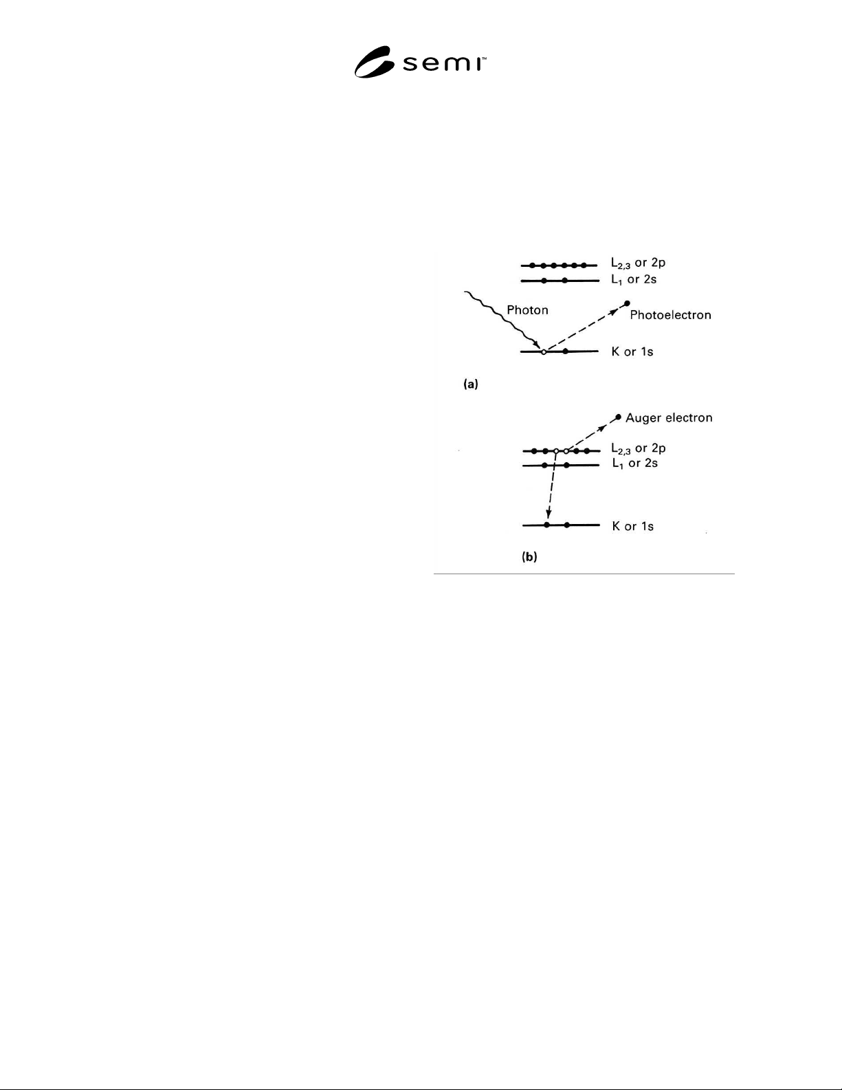
A1-1.3 In a typical ESCA instrument, a
monochromatic beam of x-rays is focused at a point of
interest on a surface. A cloud of electrons is generated
at the surface by the x-rays. This electron cloud is
made up of secondary electrons, Auger electrons and
photoelectrons. (NOTE: The generation of Auger
electrons is a byproduct of the process. If the
photoelectron was an inner shell electron, when it
leaves the atom it creates an ion in an excited state.
Once the ion is created it can de-excite via the Auger
process. The presence of Auger electrons in an ESCA
survey can be used to determine what elements were
present.) The mechanisms of ESCA photoelectron and
Auger electron generation are illustrated in Figure A1-
1.
Figure A1-1
Schematic representation of the ESCA
photoelectron and Auger electron generation
processes.
A1-1.4 An electron lens is focused at the same point as
the x-ray beam and a portion of the electron cloud
enters the lens. From the lens, the electrons enter an
electron analyzer that measures the number of electrons
as a function of their kinetic energy. The kinetic energy
is subtracted from the incident x-ray photon energy, and
the resulting binding energy is then plotted as the x-axis
with the number of electrons at each energy on the y-
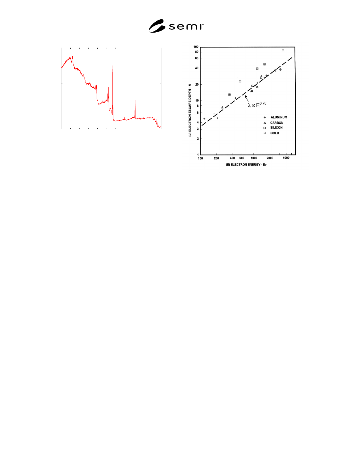
axis. An example is shown in Figure A1-2. The
binding energy can be indicative not only of the
element from which the electron came but also the
chemical bonding state of the element.
SEMI F60-0301 © SEMI 20017
Figure A1-2
Example of ESCA spectrum of the oxide passive
surface of stainless steel
A1-1.5 Illuminated Volume and Surface Sensitivity —
The incident x-ray beam penetrates well below the
surface. Photoelectrons and Auger electrons are
generated all through this illuminated volume. The
inelastic mean free path (IMFP) of an electron in a solid
is the mean distance through the solid that an electron
can travel before losing some of its energy (suffering an
inelastic interaction). The IMFP is a function of the
electron’s energy and the matrix through which it is
traveling. Electrons with an energy of approximately 1
keV have an IMFP of about 10 Å. That means that a 1
keV electron will travel, on average, 10 Å before
interacting with the matrix and giving up some of its
energy. In other words it will be scattered to lower
energy and will not be part of the photoelectron or
Auger electron line for its element. The IMFP is a
statistical parameter and an electron may travel several
IMFPs before having a collision. The “several IMFPs”
is called the escape depth of the electron, or the depth
of analysis, as shown in Figure A1-3. Although ESCA
and Auger are considered surface analytical tools, their
depth of analysis is on the order of 50 Å, or about one
to two times the depth of the oxide film found on a
typical passivated stainless steel surface.
Figure A1-3
The electron escape depth of low energy electrons in
some metals.
A1-1.6 Depth of Analysis Function — There has been
some discussion with respect to the “Depth of Analysis
Function”. There is one school that believes that it is 5
IMFPs and another that uses 3 IMFPs. These two
functions will be referred to as 5λ and 3λ respectively.
It will be seen that it makes little difference which
function is used even though the depth of the oxide
films is of the order of the functions. These functions
are seen in Figure A1-4, which shows the proportion of
the total signal generated from each depth below the
surface. The y-axis is in decimal and the x-axis is in
angstroms from the surface. The first point of the 5λ
curve is 0.16 at the 1
st
angstrom level. That means that
16% of the signal comes from the 1
st
angstrom, 14%
from the 2
nd
angstrom level and so on down to 1% from
the 25
th
angstrom level. Thus elements that do not
appear on the surface or in the first 24 angstroms in
from the surface, but do exist at the 25 Å level will be
detected.
t
rum Skip Auto by 1
010020030040050060070080090010001100
0
1
2
3
4
5
6
7
8
9
x 10
4
FCEPSSe1.spe
Binding Energy (eV)
c/s
-O KLL
-O KL
L
-Fe LMM
-Fe2p3
-Cr2p3
-O1s
-N1s
-C1s
-P2s
-P2p
-Fe3s
-Fe3p
-Cr3p
-Mo3d
-Ni LMM
-Ni3p
-Ni2p3