semi合集-English.pdf - 第7240页
SEMI MF525-0705 © SEMI 2003, 2005 3 NOTICE: Unless otherwise indicated, all documents cited shall be the latest published versions. 5 Terminology 5.1 Definitions 5.1.1 effective electrical contact radius, a (cm) — of a s…

SEMI MF525-0705 © SEMI 2003, 2005 2
3.3 Radio-Frequency Fields — Spurious currents can be introduced in the testing circuit when the equipment is
located near high-frequency generators. If equipment is located near such sources, adequate shielding must be
provided.
3.4 Mechanical Vibrations — The apparatus may be sensitive to building or other vibrations. Therefore, the probe
should be located in an area free from significant vibrations. It may be desirable to mount the probe assembly on a
vibration-free table.
3.5 Minority Carrier Injection — Caution should be taken to prevent minority carrier injection during the
measurement. Experience has shown that if the potential on the probe is kept to 20 mV or less, minority carrier
injection does not occur.
3.6 Reactive Atmosphere — Exposure of the probe or specimen to reactive atmospheres, such as those produced in
the vicinity of epitaxial reactors or by high humidity, leads to changes in the characteristics of the instrument and to
nonreproducible measurements. Probes and specimens shall be protected from such exposure. Relative humidity in
excess of 60% shall be avoided.
3.7 Semiconductor Surfaces
3.7.1 Surface Instability — It has been found that spreading resistance measurements made on surfaces that have
been exposed to an aqueous solution may be erratic. Surfaces exposed to solutions containing fluorine ions may
also exhibit instability. The heat treatment included in the procedure (see ¶13.5) may reduce these instabilities.
3.7.2 Surface Damage — Spreading resistance measurements made in areas of severe or nonuniform mechanical
damage may give erroneous results. Such damage may be caused by previous spreading resistance probe marks.
3.8 Correction Factors — When the ratio of epitaxial layer thickness, t, to the effective electrical contact radius of
the probe, a, is less than 20, it is necessary to employ correction factors to determine the correct resistivity value
from the spreading resistance measurement.
1
4 Referenced Standards and Documents
4.1 SEMI Standards
SEMI E89 — Guide for Measurement System Analysis (MSA)
SEMI M59 — Terminology for Silicon Technology
SEMI MF26 — Test Methods for Determining the Orientation of a Semiconductive Single Crystal
SEMI MF42 — Test Methods for Conductivity Type of Extrinsic Semiconducting Materials
SEMI MF84 — Test Method for Measuring Resistivity of Silicon Slices with an In-line Four-point Probe
SEMI MF95 — Test Method for Thickness of Lightly Doped Silicon Epitaxial Layers on Heavily Doped Silicon
Substrates Using an Infrared Dispersive Spectrophotometer
SEMI MF110 — Test Method for Thickness of Epitaxial or Diffused Layers in Silicon by the Angle Lapping and
Staining Technique
SEMI MF374 — Test Method for Sheet Resistance of Silicon Epitaxial, Diffused Polysilicon, and Ion-implanted
Layers Using an In-Line Four-Point Probe with the Single-configuration Procedure
SEMI MF1392 — Test Method for Determining Net Carrier Density Profiles in Silicon Wafers by Capacitance-
Voltage Measurements With a Mercury Probe
4.2 ASTM Standard
E 1 — Specification for ASTM Thermometers
2
1 Dickey, J. H., “Two-Point Probe Correction Factors,” in Semiconductor Measurement Technology: Spreading Resistance Symposium, NBS
Special Publication 400-10, December 1974, Ehrstein, J. R., Ed., pp. 4550. Available from the Superintendent of Documents, U. S. Government
Printing Office, Washington, DC 20402. SD Catalog Number C13.10:400-10.
2 Annual Book of ASTM Standards, Vol 14.03, ASTM International, 100 Barr Harbor Drive, West Conshohocken, PA 19428. Telephone: 610-
832-9500, Fax: 610-832-9555, Website:
www.astm.org
.

SEMI MF525-0705 © SEMI 2003, 2005 3
NOTICE: Unless otherwise indicated, all documents cited shall be the latest published versions.
5 Terminology
5.1 Definitions
5.1.1 effective electrical contact radius, a (cm) — of a spreading resistance probe assembly, an empirical quantity
defined by:
s
R
n
a
4
(1)
where:
n = number of current-carrying probes across which the potential drop is determined,
=
resistivity of a homogeneous semiconductor specimen, ·cm, and
R
s
=
measured spreading resistance, .
5.1.1.1 Discussion — For a three-probe arrangement, n = 1; for a two-probe arrangement, n = 2
5.1.2 epitaxial layer (in semiconconductor technology) — a layer of single crystal semiconducting material grown
on a host substrate that determines its orientation.
5.1.2.1 Discussion — A structure may consist of several epitaxial layers on a substrate: each layer is separated
from a neighboring layer (or the substrate) by an interface region.
5.1.3 spreading resistance, R
s
() — of a semiconductor, the ratio of (1) the potential drop between a small-area
conductive metal probe and a reference point on the semiconductor, to (2) the current through the probe.
5.1.3.1 Discussion — This ratio, in fact, measures metal-to-semiconductor contact resistance as well as classical
spreading resistance for a homogeneous specimen without electrical boundaries in the vicinity of the probes. For a
specimen having resistivity gradients or electrical boundaries, this ratio also includes an effect due to these gradients
or boundaries
5.1.3.2 In a three-probe arrangement, the experimental conditions approximate those of the definition (based on a
single probe) and the spreading resistance R
s
, in , is given by
I
V
R
s
(2)
where:
V = potential drop between one of the current-carrying probes and the reference (non-current carrying) probe on
the front surface, mV, and
I = current through the metal probe, mA.
In a two-probe arrangement, the potential drop, V, is measured between two similar current-carrying probes. In this
case, the voltage-to-current ratio, and hence the spreading resistance, is approximately twice that associated with a
single probe.
5.1.4 substrate (in semiconductor technology) — a wafer that is the basis for subsequent processing operations in
the fabrication of semiconductor devices or circuits.
5.1.4.1 Discussion — The devices or circuits may be fabricated directly in the substrate or in a film of the same or
another material grown or deposited on the substrate..
5.1.5 Other terms relating to silicon technology are defined in SEMI M59.
5.1.6 Terms related to measurement precision are defined in SEMI E89.
6 Summary of Test Method
6.1 The spreading resistance of a reproducibly formed point contact is measured.
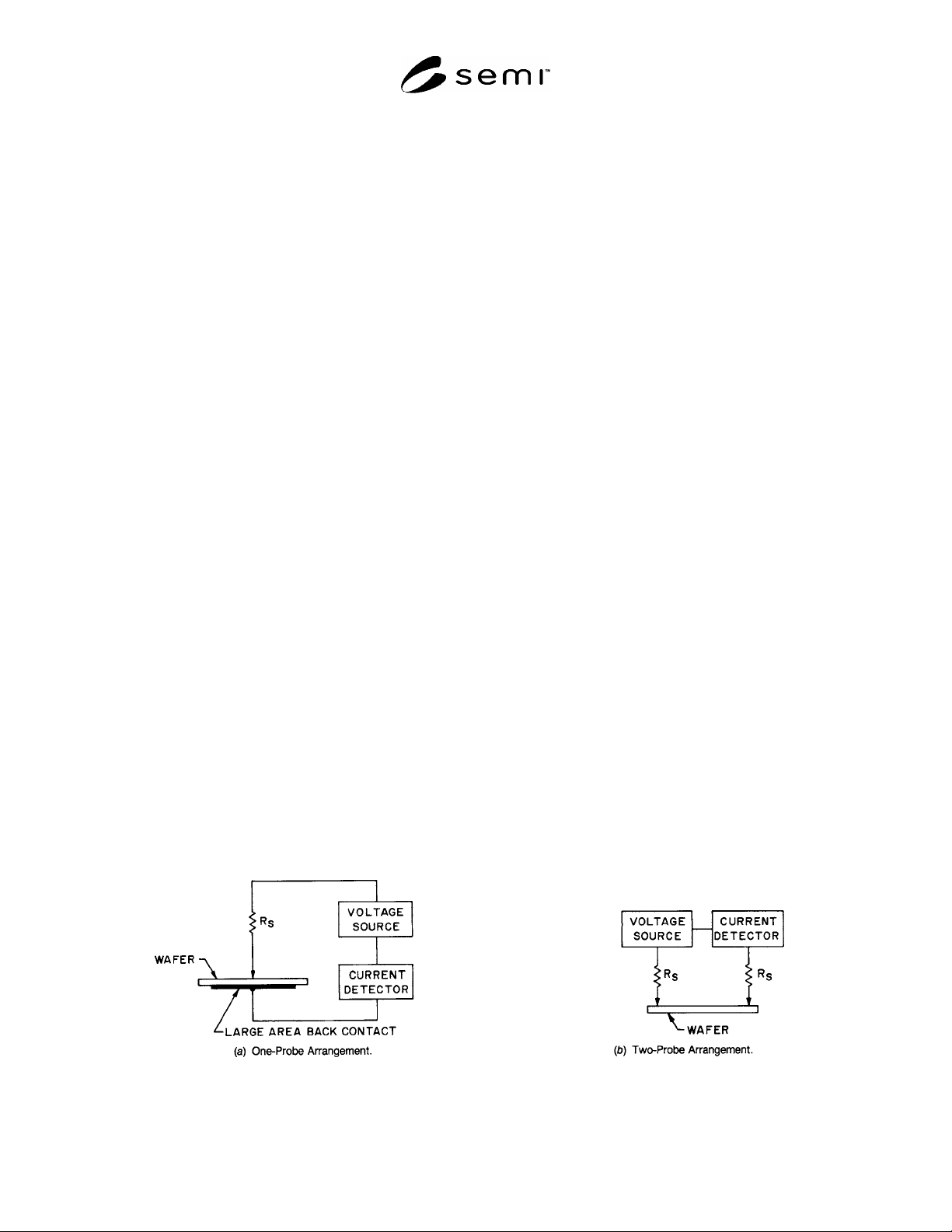
SEMI MF525-0705 © SEMI 2003, 2005 4
6.2 The resistivity of the material in the vicinity of the probe is determined from a calibration curve derived from
spreading resistance measurements made under the same conditions on reference specimens of known resistivity.
6.3 The spreading resistance may be measured with the use of one, two, or three probes and (1) by applying a
known constant voltage and measuring the current, (2) by applying a known constant current and measuring the
voltage, or (3) by a resistance comparator technique.
7 Apparatus
7.1 Mechanical Apparatus
7.1.1 Probes and Probe Assembly — A spreading resistance probe assembly with provision for supporting and
lowering either one, two, or three replaceable probe tips to the wafer surface at a reproducible rate and with a
predetermined load. The supporting mechanism shall provide for spatial displacement of the probes for adjustment
of the point of contact.
7.1.1.1 Probe Tip Material — A hard, durable, low-resistance substance that wears well without flaking, such as
osmium, tungsten carbide, or tungsten-ruthenium alloys.
7.1.1.2 Probe Tip Radius — The mechanical radius of curvature of the probe tips in the region that will touch the
specimen shall be less than or equal to 25 m. The tip angle of the probe shall be within the range from 30 to 60°,
inclusive.
7.1.1.3 Probe Loading and Descent Rate — The loading applied to each point shall be less than 50 gf (490 mN).
A 1-mm/s descent rate has been found to be adequate for a 40 gf (390 mN) load (see ¶11.3 and Note 5).
7.1.1.4 Probe Spacing — as used for calibration (see §15).
NOTE 1: Typical probe spacings are between 15 and 1000 m.
7.1.1.5 Probe Insulation — A d-c isolation resistance of 1 G or greater between any pair of probes and between
each probe and any guard circuit used.
7.1.2 Sample Holder — An insulated vacuum chuck or other means for clamping the substrate tightly while
measurements are made.
NOTE 2: The vacuum chuck may be inserted on a high-resolution translatable microscope stage with drum calibrated preferably
in metric units. Gear boxes for stage movement should allow step-size movements in the range from 5 to 500 m per step,
inclusive. Usual increments are 5.0, 10, 25, and multiples of 10 thereof.
7.2 Electrical Measuring Apparatus
7.2.1 Constant-Voltage Method — Suitable for use with the one- or two-probe arrangement. See Figure 1.
7.2.1.1 D-C Voltage Source — With a constant output between 1 and 20 mV, inclusive. The output potential shall
be constant to within ±0.1% into a load that varies from 1 to 10 M, inclusive.
7.2.1.2 D-C Current Detector — Accurate to within ±0.1% and capable of covering the range from 10 mA to 1 pA,
inclusive.
Figure 1
Electrical Circuits for the Constant-Voltage Method